


Si53xx-RM
Rev. 0.52
25
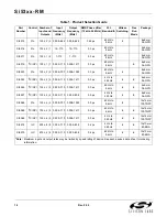
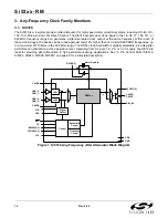
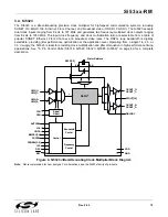
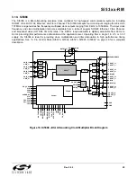
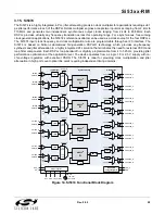
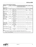
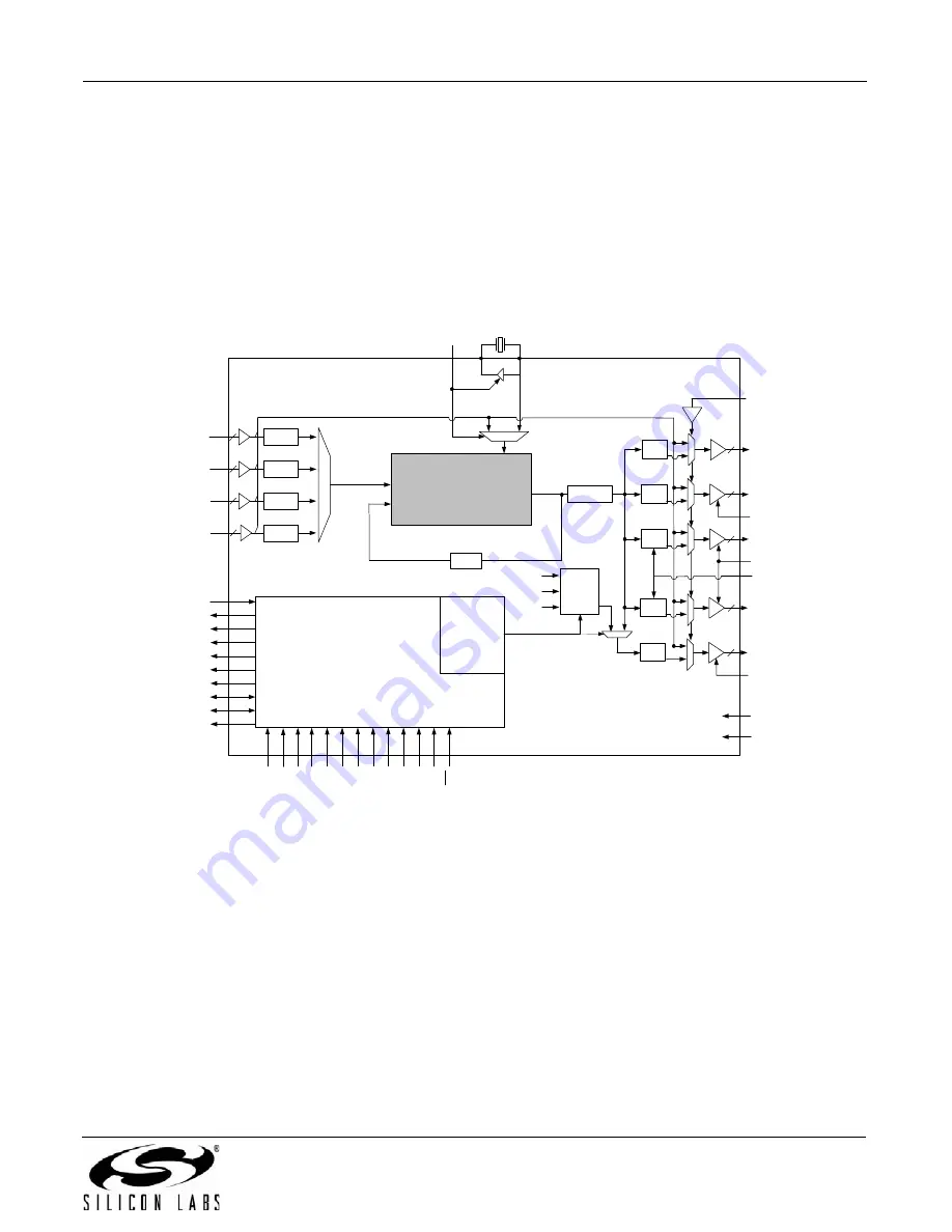
3.10. Si5366
The Si5366 is a jitter-attenuating precision clock multiplier for high-speed communication systems, including
SONET OC-48/OC-192, Ethernet, and Fibre Channel. The Si5366 accepts four clock inputs ranging from 8 kHz to
707 MHz and generates five frequency-multiplied clock outputs ranging from 8 kHz to 1050 MHz. The input clock
frequency and clock multiplication ratio are selectable from a table of popular SONET, Ethernet, Fibre Channel,
and broadcast video (HD SDI, 3G SDI) rates. The DSPLL loop bandwidth is digitally selectable from 60 Hz to
8 kHz, providing jitter performance optimization at the application level. Operating from a single 1.8, 2.5, or 3.3 V
supply, the Si5366 is ideal for providing clock multiplication and jitter attenuation in high performance timing
applications. See "6. Pin Control Parts (Si5316, Si5322, Si5323, Si5365, Si5366)" on page 49 for a complete
description.
Figure 10. Si5366 Jitter Attenuating Clock Multiplier Block Diagram
C2A
CS0_C3A
C2B
CS1_C4A
ALRMOUT
C1A
CKIN_1–
CKIN_2–
C3B
CKIN_3–
CKIN_4–
C1B
CKIN_3
CKIN_4
CKOUT_2
VDD
GND
CKOUT_1–
÷ NC1
1
0
CKOUT_2–
÷ NC2
1
0
CKOUT_3–
÷ NC3
1
0
CKOUT_4–
÷ NC4
1
0
2
2
2
2
2
2
2
2
f
OSC
Xtal or Refclock
RATE[1:0]
XA
XB
f
x
f
3
DBL2_BY
DBL34
DBL5
FSYNC
LOGIC/
ALIGN
CK_CONF
BWS
E
L[
1:
0]
FR
Q
S
E
L
[3:
0]
DI
V
3
4
[1:
0]
FOS
_
CT
L
SFO
UT
[1:
0
]
INC
DEC
FS
_SW
FS_AL
IGN
RST
CM
O
D
E
AUTOSEL
BYPASS/DSBL2
LOL
Control
÷ N3_2
÷ N3_1
FSYNC
3
÷ N3_3
÷ N3_4
CKOUT_5–
÷ NC5
1
0
2
1
0
FRQTBL
DIV34[1:0]
÷ N1_HS
DSPLL
®
÷ N2
Summary of Contents for Si5316 Series
Page 2: ...Si53xx RM 2 Rev 0 52 ...
Page 110: ...Si53xx RM 110 Rev 0 52 Figure 48 sfout_5 LVPECL Figure 49 sfout_6 CML ...
Page 111: ...Si53xx RM Rev 0 52 111 Figure 50 sfout_7 LVDS ...
Page 127: ...Si53xx RM Rev 0 52 127 Figure 66 155 52 MHz In 622 08 MHz Out Loop BW 7 Hz Si5324 ...
Page 128: ...Si53xx RM 128 Rev 0 52 Figure 67 19 44 MHz In 156 25 MHz Out Loop BW 80 Hz ...
Page 129: ...Si53xx RM Rev 0 52 129 Figure 68 19 44 MHz In 156 25 MHz Out Loop BW 5 Hz Si5324 ...
Page 131: ...Si53xx RM Rev 0 52 131 Figure 70 61 44 MHz In 491 52 MHz Out Loop BW 7 Hz Si5324 ...
Page 132: ...Si53xx RM 132 Rev 0 52 Figure 71 622 08 MHz In 672 16 MHz Out Loop BW 6 9 kHz ...
Page 133: ...Si53xx RM Rev 0 52 133 Figure 72 622 08 MHz In 672 16 MHz Out Loop BW 100 Hz ...
Page 134: ...Si53xx RM 134 Rev 0 52 Figure 73 156 25 MHz In 155 52 MHz Out ...
Page 139: ...Si53xx RM Rev 0 52 139 Figure 78 86 685 MHz In 173 371 MHz Out ...
Page 140: ...Si53xx RM 140 Rev 0 52 Figure 79 86 685 MHz In 693 493 MHz Out ...
Page 142: ...Si53xx RM 142 Rev 0 52 Figure 81 10 MHz In 1 GHz Out ...
Page 174: ...Si53xx RM 174 Rev 0 52 Figure 99 Si5374 Si5375 DSPLL A ...
Page 175: ...Si53xx RM Rev 0 52 175 Figure 100 Si5374 Si5375 DSPLL B ...
Page 176: ...Si53xx RM 176 Rev 0 52 Figure 101 Si5374 Si5375 DSPLL C ...