


Si53xx-RM
Rev. 0.52
31
4. Device Specifications
The following tables are intended to simplify device selection. The specifications in the individual device data
sheets take precedence over this document. Refer to the respective device data sheet for devices not listed in the
tables below.
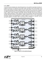
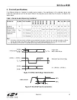
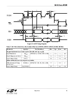
Figure 16. Differential Voltage Characteristics
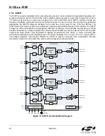
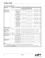
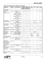
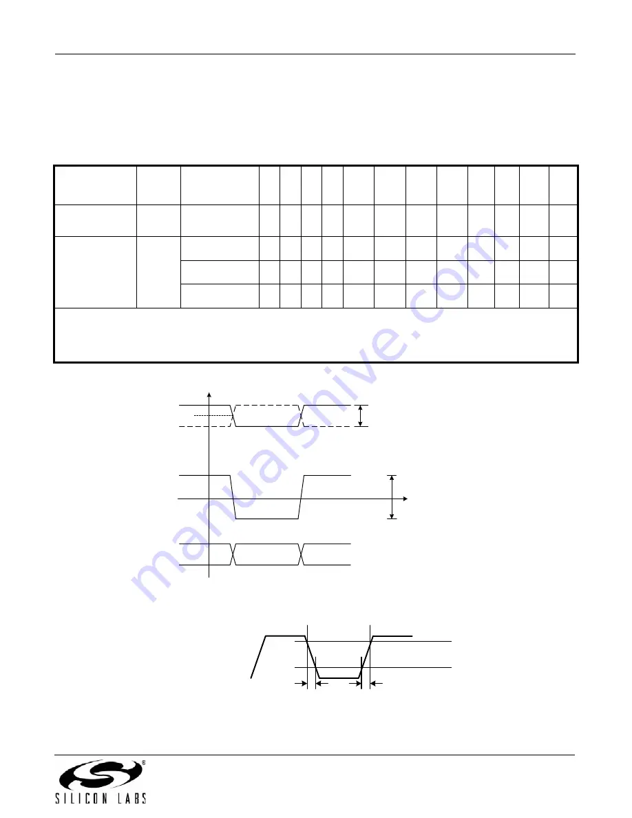
Figure 17. Rise/Fall Time Characteristics
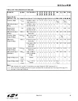
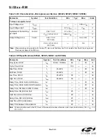
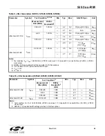
Table 3. Recommended Operating Conditions
1
Parameter
Symbol Test Condition
Si53
16
Si53
22
Si53
24
Si53
25
Si53
65
Si53
66
Si53
67
Si53
68
Min Typ Max Unit
Ambient
Temperature
T
A
–40
25
85
ºC
Supply Voltage
During Normal
Operation
V
DD
3.3 V Nominal
Note 2 Note 2 Note 2 Note 2
2.97 3.3
3.63
V
2.5 V Nominal
2.25 2.5
2.75
V
1.8 V Nominal
1.71 1.8
1.89
V
Note:
1.
All minimum and maximum specifications are guaranteed and apply across the recommended operating conditions.
Typical values apply at nominal supply voltages and an operating temperature of 25 ºC unless otherwise stated.
2.
See Sections 6.7.1 and 8.2.1 for restrictions on output formats for TQFP devices at 3.3 V.
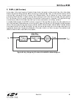
V
ISE
, V
OSE
V
ID
,V
OD
Differential I/Os
V
ICM
, V
OCM
Single-Ended
Peak-to-Peak Voltage
Differential Peak-to-Peak Voltage
SIGNAL –
() – (SIGNAL –)
V
t
SIGNAL –
V
ID
= () – (SIGNAL–)
V
ICM
, V
OCM
t
F
t
R
80%
20%
CKIN, CKOUT
Summary of Contents for Si5316 Series
Page 2: ...Si53xx RM 2 Rev 0 52 ...
Page 110: ...Si53xx RM 110 Rev 0 52 Figure 48 sfout_5 LVPECL Figure 49 sfout_6 CML ...
Page 111: ...Si53xx RM Rev 0 52 111 Figure 50 sfout_7 LVDS ...
Page 127: ...Si53xx RM Rev 0 52 127 Figure 66 155 52 MHz In 622 08 MHz Out Loop BW 7 Hz Si5324 ...
Page 128: ...Si53xx RM 128 Rev 0 52 Figure 67 19 44 MHz In 156 25 MHz Out Loop BW 80 Hz ...
Page 129: ...Si53xx RM Rev 0 52 129 Figure 68 19 44 MHz In 156 25 MHz Out Loop BW 5 Hz Si5324 ...
Page 131: ...Si53xx RM Rev 0 52 131 Figure 70 61 44 MHz In 491 52 MHz Out Loop BW 7 Hz Si5324 ...
Page 132: ...Si53xx RM 132 Rev 0 52 Figure 71 622 08 MHz In 672 16 MHz Out Loop BW 6 9 kHz ...
Page 133: ...Si53xx RM Rev 0 52 133 Figure 72 622 08 MHz In 672 16 MHz Out Loop BW 100 Hz ...
Page 134: ...Si53xx RM 134 Rev 0 52 Figure 73 156 25 MHz In 155 52 MHz Out ...
Page 139: ...Si53xx RM Rev 0 52 139 Figure 78 86 685 MHz In 173 371 MHz Out ...
Page 140: ...Si53xx RM 140 Rev 0 52 Figure 79 86 685 MHz In 693 493 MHz Out ...
Page 142: ...Si53xx RM 142 Rev 0 52 Figure 81 10 MHz In 1 GHz Out ...
Page 174: ...Si53xx RM 174 Rev 0 52 Figure 99 Si5374 Si5375 DSPLL A ...
Page 175: ...Si53xx RM Rev 0 52 175 Figure 100 Si5374 Si5375 DSPLL B ...
Page 176: ...Si53xx RM 176 Rev 0 52 Figure 101 Si5374 Si5375 DSPLL C ...


