


Si53xx-RM
Rev. 0.52
33
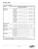
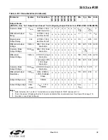
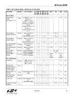
Output Clocks
(CKOUTn—See “8.2. Output Clock Drivers” for Configuring Output Drivers for LVPECL/CML/LVDS/CMOS)
Common Mode
V
OCM
LVPECL 100
load line-to-line
V
DD
–
1.42
—
V
DD
–
1.25
V
Differential Output
Swing
V
OD
LVPECL 100
load line-to-line
1
1.1
—
1.9
V
PP
Single Ended
Output Swing
V
SE
LVPECL 100
load line-to-line
1
0.5
—
0.93
V
PP
Differential Output
Voltage
CKO
VD
CML 100
load
line-to-line
350
425
500
mV
PP
Common Mode
Output Voltage
CKO
VCM
CML 100
load
line-to-line
—
V
DD
– .36
—
V
Differential
Output Voltage
CKO
VD
LVDS 100
load
line-to-line
500
700
900
mV
PP
Low swing LVDS
100
load
line-to-line
350
425
500
mV
PP
Common Mode
Output Voltage
CKO
VCM
LVDS 100
load
line-to-line
1.125
1.2
1.275
V
Differential Output
Resistance
CKO
RD
CML, LVPECL,
LVDS, Disabled,
Sleep
170
200
230
Output Voltage Low
CKO-
VOLLH
CMOS
—
—
0.4
V
Output Voltage High
CKO-
VOHLH
V
DD
= 1.71 V
CMOS
0.8 x
V
DD
—
—
V
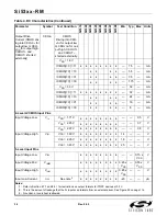
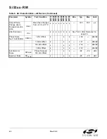
Table 4. DC Characteristics (Continued)
Parameter
Symbol
Test Condition
Si5
316
Si5
322
Si5
324
Si5
325
Si5
365
Si5
366
Si5
367
Si5
368
Min
Typ
Max
Units
Notes:
1.
Refer to Section 6.7.1 and 8.2.1 for restrictions on output formats for TQFP devices at 3.3 V.
2.
This is the amount of leakage that the 3L inputs can tolerate from an external driver. See Figure 55 on page 114.
3.
No under- or overshoot is allowed.
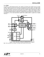
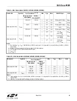
Summary of Contents for Si5316 Series
Page 2: ...Si53xx RM 2 Rev 0 52 ...
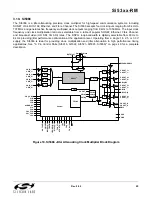
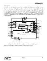
Page 110: ...Si53xx RM 110 Rev 0 52 Figure 48 sfout_5 LVPECL Figure 49 sfout_6 CML ...
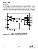
Page 111: ...Si53xx RM Rev 0 52 111 Figure 50 sfout_7 LVDS ...
Page 127: ...Si53xx RM Rev 0 52 127 Figure 66 155 52 MHz In 622 08 MHz Out Loop BW 7 Hz Si5324 ...
Page 128: ...Si53xx RM 128 Rev 0 52 Figure 67 19 44 MHz In 156 25 MHz Out Loop BW 80 Hz ...
Page 129: ...Si53xx RM Rev 0 52 129 Figure 68 19 44 MHz In 156 25 MHz Out Loop BW 5 Hz Si5324 ...
Page 131: ...Si53xx RM Rev 0 52 131 Figure 70 61 44 MHz In 491 52 MHz Out Loop BW 7 Hz Si5324 ...
Page 132: ...Si53xx RM 132 Rev 0 52 Figure 71 622 08 MHz In 672 16 MHz Out Loop BW 6 9 kHz ...
Page 133: ...Si53xx RM Rev 0 52 133 Figure 72 622 08 MHz In 672 16 MHz Out Loop BW 100 Hz ...
Page 134: ...Si53xx RM 134 Rev 0 52 Figure 73 156 25 MHz In 155 52 MHz Out ...
Page 139: ...Si53xx RM Rev 0 52 139 Figure 78 86 685 MHz In 173 371 MHz Out ...
Page 140: ...Si53xx RM 140 Rev 0 52 Figure 79 86 685 MHz In 693 493 MHz Out ...
Page 142: ...Si53xx RM 142 Rev 0 52 Figure 81 10 MHz In 1 GHz Out ...
Page 174: ...Si53xx RM 174 Rev 0 52 Figure 99 Si5374 Si5375 DSPLL A ...
Page 175: ...Si53xx RM Rev 0 52 175 Figure 100 Si5374 Si5375 DSPLL B ...
Page 176: ...Si53xx RM 176 Rev 0 52 Figure 101 Si5374 Si5375 DSPLL C ...


