


S i 5 3 x x - R M
36
Rev. 0.52
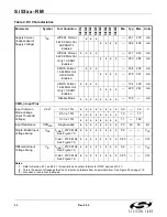
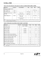
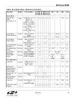
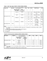
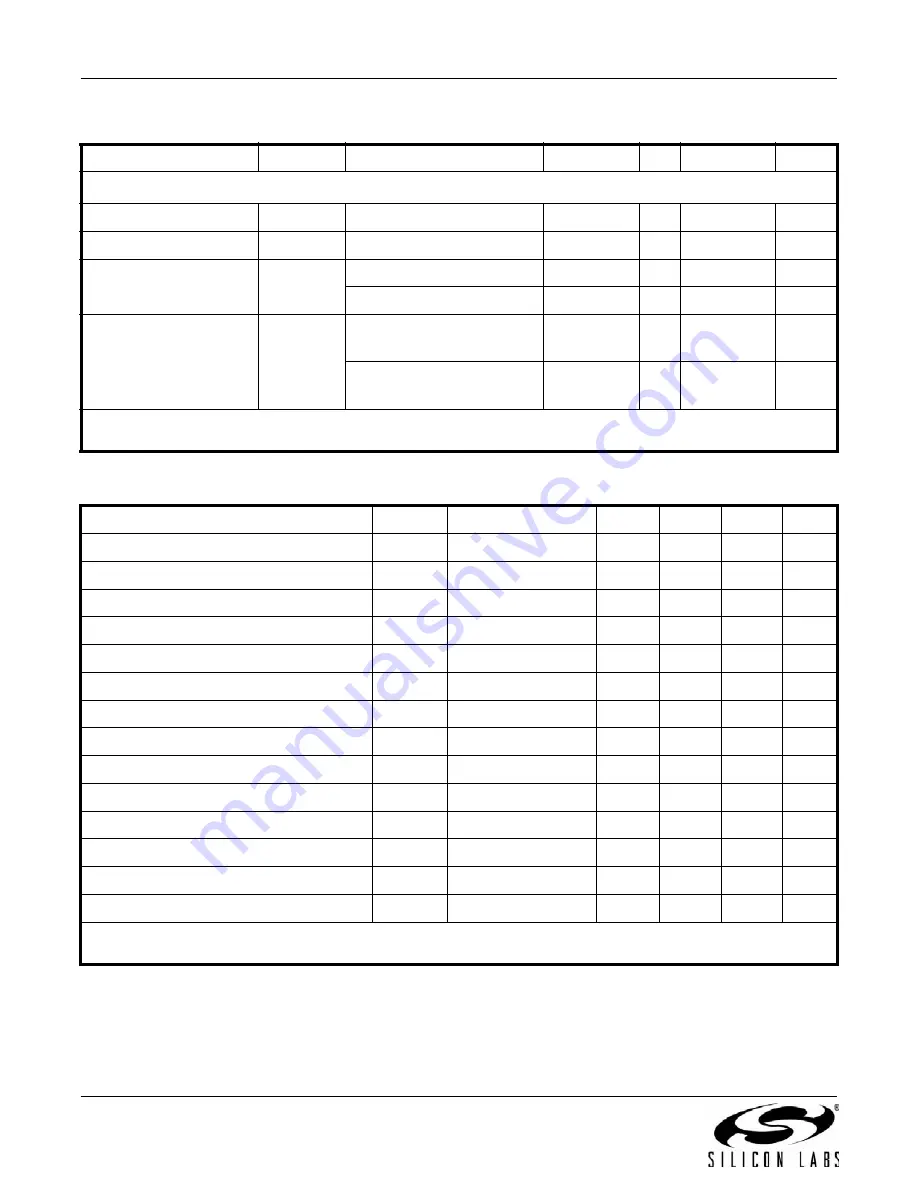
Table 5. DC Characteristics—Microprocessor Devices (Si5324, Si5325, Si5367, Si5368)
Parameter
Symbol
Test Condition
Min
Typ
Max
Units
I
2
C Bus Lines (SDA, SCL)*
Input Voltage Low
V
ILI2C
—
—
0.25 x V
DD
V
Input Voltage High
V
IHI2C
0.7 x V
DD
—
V
DD
V
Hysteresis of Schmitt trig-
ger inputs
V
HYSI2C
V
DD
= 1.8 V
0.1 x V
DD
—
—
V
V
DD
= 2.5 or 3.3 V
0.05 x V
DD
—
—
V
Output Voltage Low
V
OHI2C
V
DD
= 1.8 V
IO = 3 mA
—
—
0.2 x V
DD
V
V
DD
= 2.5 or 3.3 V
IO = 3 mA
—
—
0.4
V
*Note:
When selecting pull-up resistors for the two I
2
C pins, note that there is a 75 k
resistor from the SCL pin to ground.
This does not apply to the SDA pin.
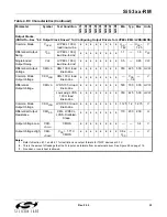
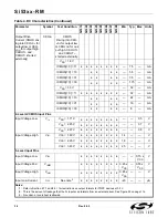
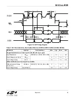
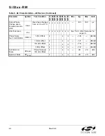
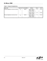
Table 6. SPI Specifications (Si5324, Si5325, Si5367, and Si5368)
Parameter
Symbol
Test Conditions
Min
Typ
Max
Unit
Duty Cycle, SCLK
t
DC
SCLK = 10 MHz
40
—
60
%
Cycle Time, SCLK
t
c
100
—
—
ns
Rise Time, SCLK
t
r
20–80%
—
—
25
ns
Fall Time, SCLK
t
f
20–80%
—
—
25
ns
Low Time, SCLK
t
lsc
20–20%
30
—
—
ns
High Time, SCLK
t
hsc
80–80%
30
—
—
ns
Delay Time, SCLK Fall to SDO Active
t
d1
—
—
25
ns
Delay Time, SCLK Fall to SDO Transition
t
d2
—
—
25
ns
Delay Time, SS Rise to SDO Tri-state
t
d3
—
—
25
ns
Setup Time, SS to SCLK Fall
t
su1
25
—
—
ns
Hold Time, SS to SCLK Rise
t
h1
20
—
—
ns
Setup Time, SDI to SCLK Rise
t
su2
25
—
—
ns
Hold Time, SDI to SCLK Rise
t
h2
20
—
—
ns
Delay Time between Slave Selects
t
cs
25
—
—
ns
Note:
All timing is referenced to the 50% level of the waveform unless otherwise noted. Input test levels are VIH = V
DD
– 4 V,
VIL = 0.4 V.
Summary of Contents for Si5316 Series
Page 2: ...Si53xx RM 2 Rev 0 52 ...
Page 110: ...Si53xx RM 110 Rev 0 52 Figure 48 sfout_5 LVPECL Figure 49 sfout_6 CML ...
Page 111: ...Si53xx RM Rev 0 52 111 Figure 50 sfout_7 LVDS ...
Page 127: ...Si53xx RM Rev 0 52 127 Figure 66 155 52 MHz In 622 08 MHz Out Loop BW 7 Hz Si5324 ...
Page 128: ...Si53xx RM 128 Rev 0 52 Figure 67 19 44 MHz In 156 25 MHz Out Loop BW 80 Hz ...
Page 129: ...Si53xx RM Rev 0 52 129 Figure 68 19 44 MHz In 156 25 MHz Out Loop BW 5 Hz Si5324 ...
Page 131: ...Si53xx RM Rev 0 52 131 Figure 70 61 44 MHz In 491 52 MHz Out Loop BW 7 Hz Si5324 ...
Page 132: ...Si53xx RM 132 Rev 0 52 Figure 71 622 08 MHz In 672 16 MHz Out Loop BW 6 9 kHz ...
Page 133: ...Si53xx RM Rev 0 52 133 Figure 72 622 08 MHz In 672 16 MHz Out Loop BW 100 Hz ...
Page 134: ...Si53xx RM 134 Rev 0 52 Figure 73 156 25 MHz In 155 52 MHz Out ...
Page 139: ...Si53xx RM Rev 0 52 139 Figure 78 86 685 MHz In 173 371 MHz Out ...
Page 140: ...Si53xx RM 140 Rev 0 52 Figure 79 86 685 MHz In 693 493 MHz Out ...
Page 142: ...Si53xx RM 142 Rev 0 52 Figure 81 10 MHz In 1 GHz Out ...
Page 174: ...Si53xx RM 174 Rev 0 52 Figure 99 Si5374 Si5375 DSPLL A ...
Page 175: ...Si53xx RM Rev 0 52 175 Figure 100 Si5374 Si5375 DSPLL B ...
Page 176: ...Si53xx RM 176 Rev 0 52 Figure 101 Si5374 Si5375 DSPLL C ...