


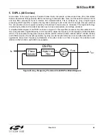


Si53xx-RM
Rev. 0.52
37
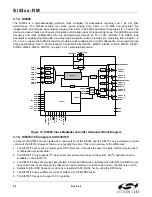
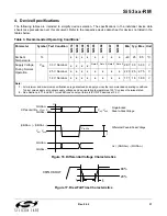
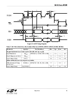
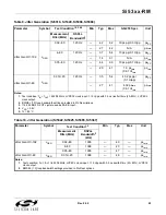
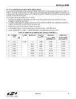
Figure 18. SPI Timing Diagram
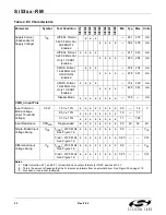
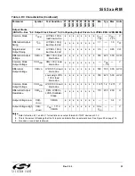
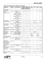
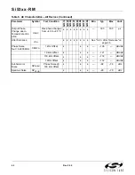
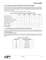
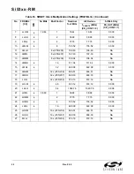
Table 7. DC Characteristics—Narrowband Devices (Si5316, Si5319, Si5323, Si5366, Si5368)
Parameter
Symbol
Test Condition
Min
Typ
Max
Unit
Single-Ended Reference Clock Input Pin XA (XB with cap to gnd)
Input Resistance
XA
RIN
(RATE[1:0] = LM, ML, MH, or HM)
—
10
—
k
Input Voltage Level Limits
XA
VIN
0
—
1.2
V
Input Voltage Swing
XA
VPP
0.5
—
1.2
V
PP
Differential Reference Clock Input Pins (XA/XB)
Differential Input Voltage
Level Limits
XA/XB
VIN
(RATE[1:0] = LM, ML, MH, or HM)
0
—
1.2
V
Input Voltage Swing
XA
VPP
/XB
VPP
0.5
—
2.4
V
PP
SCLK
SS
SDI
t
h1
t
d3
SDO
t
d1
t
d2
t
su1
t
r
t
f
t
c
t
su2
t
h2
t
cs
t
lsc
t
hsc
Summary of Contents for Si5316 Series
Page 2: ...Si53xx RM 2 Rev 0 52 ...
Page 110: ...Si53xx RM 110 Rev 0 52 Figure 48 sfout_5 LVPECL Figure 49 sfout_6 CML ...
Page 111: ...Si53xx RM Rev 0 52 111 Figure 50 sfout_7 LVDS ...
Page 127: ...Si53xx RM Rev 0 52 127 Figure 66 155 52 MHz In 622 08 MHz Out Loop BW 7 Hz Si5324 ...
Page 128: ...Si53xx RM 128 Rev 0 52 Figure 67 19 44 MHz In 156 25 MHz Out Loop BW 80 Hz ...
Page 129: ...Si53xx RM Rev 0 52 129 Figure 68 19 44 MHz In 156 25 MHz Out Loop BW 5 Hz Si5324 ...
Page 131: ...Si53xx RM Rev 0 52 131 Figure 70 61 44 MHz In 491 52 MHz Out Loop BW 7 Hz Si5324 ...
Page 132: ...Si53xx RM 132 Rev 0 52 Figure 71 622 08 MHz In 672 16 MHz Out Loop BW 6 9 kHz ...
Page 133: ...Si53xx RM Rev 0 52 133 Figure 72 622 08 MHz In 672 16 MHz Out Loop BW 100 Hz ...
Page 134: ...Si53xx RM 134 Rev 0 52 Figure 73 156 25 MHz In 155 52 MHz Out ...
Page 139: ...Si53xx RM Rev 0 52 139 Figure 78 86 685 MHz In 173 371 MHz Out ...
Page 140: ...Si53xx RM 140 Rev 0 52 Figure 79 86 685 MHz In 693 493 MHz Out ...
Page 142: ...Si53xx RM 142 Rev 0 52 Figure 81 10 MHz In 1 GHz Out ...
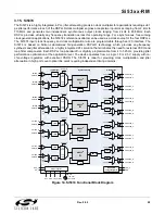
Page 174: ...Si53xx RM 174 Rev 0 52 Figure 99 Si5374 Si5375 DSPLL A ...
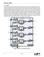
Page 175: ...Si53xx RM Rev 0 52 175 Figure 100 Si5374 Si5375 DSPLL B ...
Page 176: ...Si53xx RM 176 Rev 0 52 Figure 101 Si5374 Si5375 DSPLL C ...


