


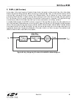


Si53xx-RM
Rev. 0.52
39
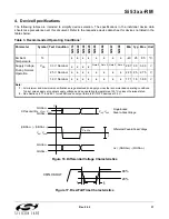
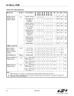
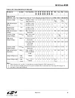
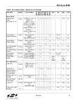
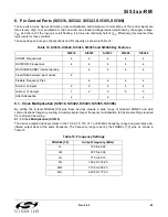
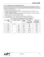
Table 8. AC Characteristics—All Devices
Parameter
Symbol
Test Condition
Si53
16
Si53
22
Si53
24
Si53
25
Si53
65
Si53
66
Si53
67
Si53
68
Min
Typ
Max
Units
Input Frequency
CKN
F
19.38
—
710
MHz
19.43
—
707.35
MHz
0.002
—
707.35
MHz
10
—
710
MHz
When used as frame
synchronization input
—
0.008
—
MHz
2
—
512
kHz
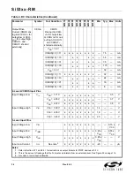
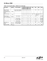
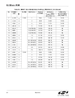
CKIN_n Input Pins
Input Duty Cycle
(Minimum Pulse
Width)
CKN
DC
Whichever is smaller
(i.e., the 40% / 60 %
limitation applies only
to high frequency
clocks) , N3 > 1
40
—
60
%
2
—
—
ns
Input Capacitance
CKN
CIN
—
—
3
pF
Input Rise/Fall
Time
CKN
TRF
20–80%
See Figure 17
—
—
11
ns
CKOUT_n Output Pins (See individual data sheets for speed grade limits)
Output Frequency
(Output not
configured for
CMOS or tri-state)
CK
OF
19.38
—
710
MHz
19.43
—
1049
MHz
0.008
—
1049
MHz
10
—
945
MHz
0.002
—
945
MHz
970
—
1134
MHz
1.213
—
1.4
GHz
Maximum Output
Frequency in
CMOS Format
CKO
FMC
—
—
212.5
MHz
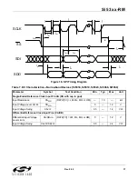
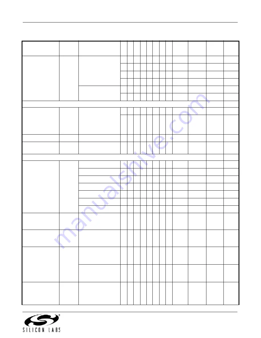
Output Rise/Fall
(20–80%) at
622.08 MHz
CKO
TRF
Output not config-
ured for CMOS See
Figure 17
—
230
350
ps
Output Rise/Fall
(20–80%) at
212.5 MHz
CKO
TRF
CMOS Output
V
DD
= 1.62
Cload = 5 pF
—
—
8
ns
CMOS Output
V
DD
= 2.97
Cload = 5 pF
—
—
2
ns
Output Duty Cycle
Differential
Uncertainty
CKO
DC
100
Load
Line to Line
Measured at 50%
Point (not for CMOS)
—
—
±40
ps
Summary of Contents for Si5316 Series
Page 2: ...Si53xx RM 2 Rev 0 52 ...
Page 110: ...Si53xx RM 110 Rev 0 52 Figure 48 sfout_5 LVPECL Figure 49 sfout_6 CML ...
Page 111: ...Si53xx RM Rev 0 52 111 Figure 50 sfout_7 LVDS ...
Page 127: ...Si53xx RM Rev 0 52 127 Figure 66 155 52 MHz In 622 08 MHz Out Loop BW 7 Hz Si5324 ...
Page 128: ...Si53xx RM 128 Rev 0 52 Figure 67 19 44 MHz In 156 25 MHz Out Loop BW 80 Hz ...
Page 129: ...Si53xx RM Rev 0 52 129 Figure 68 19 44 MHz In 156 25 MHz Out Loop BW 5 Hz Si5324 ...
Page 131: ...Si53xx RM Rev 0 52 131 Figure 70 61 44 MHz In 491 52 MHz Out Loop BW 7 Hz Si5324 ...
Page 132: ...Si53xx RM 132 Rev 0 52 Figure 71 622 08 MHz In 672 16 MHz Out Loop BW 6 9 kHz ...
Page 133: ...Si53xx RM Rev 0 52 133 Figure 72 622 08 MHz In 672 16 MHz Out Loop BW 100 Hz ...
Page 134: ...Si53xx RM 134 Rev 0 52 Figure 73 156 25 MHz In 155 52 MHz Out ...
Page 139: ...Si53xx RM Rev 0 52 139 Figure 78 86 685 MHz In 173 371 MHz Out ...
Page 140: ...Si53xx RM 140 Rev 0 52 Figure 79 86 685 MHz In 693 493 MHz Out ...
Page 142: ...Si53xx RM 142 Rev 0 52 Figure 81 10 MHz In 1 GHz Out ...
Page 174: ...Si53xx RM 174 Rev 0 52 Figure 99 Si5374 Si5375 DSPLL A ...
Page 175: ...Si53xx RM Rev 0 52 175 Figure 100 Si5374 Si5375 DSPLL B ...
Page 176: ...Si53xx RM 176 Rev 0 52 Figure 101 Si5374 Si5375 DSPLL C ...


