


Si53xx-RM
Rev. 0.52
41
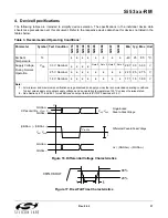
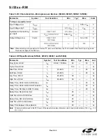
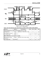
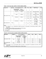
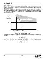
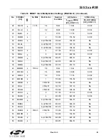
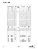
Device Skew
Output Clock
Skew,
see Section 7.7.4
t
SKEW
of CKOUT_n to
of
CKOUT_m,
CKOUT_n and
CKOUT_m at same
frequency and signal
format
PHASE OFFSET = 0
SQICAL = 1
CKOUT_ALWAYS_O
N = 1
—
—
100
ps
Coarse Skew
Adjust Resolution
t
PHRES
Using
CLAT
[7:0]
register
—
1/F
VCO
—
ps
using INC/DEC pins
—
1/F
VCO
—
ps
Coarse Skew
Adjust Range
t
PHSRNG
Using
CLAT
[7:0]
register
–
—
+
using INC/DEC pins
–
—
+
s
Fine Skew Adjust
Resolution
t
FPHSRES
using
FLAT
[14:0]
register
—
9
—
ps
Fine Skew Adjust
Range
t
FPHSRNG
using
FLAT
[14:0]
register
–110
—
110
ps
Phase Offset
Resolution
t
OFSTRES
using
PHASEOFF-
SETn
[7:0] registers
—
N1_HS/
f
VCO
—
Phase Offset
Range
t
OFSTRNG
using
PHASEOFF-
SETn
[7:0] registers
–128 x
t
OF-
STRES
—
127 x
t
OF-
STRES
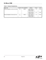
PLL Performance
Lock Time
t
LOCKHW
RST with valid
CKIN to
LOL;
BW = 100 Hz
—
1.2
sec
Pin Reset or
Register Reset to
Microprocessor
Access Ready
t
READY
—
—
10
ms
Reset to first
on
CKOUT
t
START
Valid, stable clock on
CKIN
—
—
1.2
sec
Minimum Reset
Pulse Width
t
RSTMIN
1
—
—
µs
Lock Time
t
LOCKMP
Start of ICAL to
of
LOL,
lowest BW setting
—
35
1000
ms
Closed Loop Jitter
Peaking
J
PK
—
0.05
0.1
dB
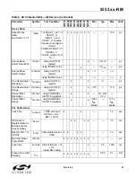
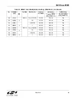
Table 8. AC Characteristics—All Devices (Continued)
Parameter
Symbol
Test Condition
Si5
316
Si5
322
Si5
324
Si5
325
Si5
365
Si5
366
Si5
367
Si5
368
Min
Typ
Max
Units
Summary of Contents for Si5316 Series
Page 2: ...Si53xx RM 2 Rev 0 52 ...
Page 110: ...Si53xx RM 110 Rev 0 52 Figure 48 sfout_5 LVPECL Figure 49 sfout_6 CML ...
Page 111: ...Si53xx RM Rev 0 52 111 Figure 50 sfout_7 LVDS ...
Page 127: ...Si53xx RM Rev 0 52 127 Figure 66 155 52 MHz In 622 08 MHz Out Loop BW 7 Hz Si5324 ...
Page 128: ...Si53xx RM 128 Rev 0 52 Figure 67 19 44 MHz In 156 25 MHz Out Loop BW 80 Hz ...
Page 129: ...Si53xx RM Rev 0 52 129 Figure 68 19 44 MHz In 156 25 MHz Out Loop BW 5 Hz Si5324 ...
Page 131: ...Si53xx RM Rev 0 52 131 Figure 70 61 44 MHz In 491 52 MHz Out Loop BW 7 Hz Si5324 ...
Page 132: ...Si53xx RM 132 Rev 0 52 Figure 71 622 08 MHz In 672 16 MHz Out Loop BW 6 9 kHz ...
Page 133: ...Si53xx RM Rev 0 52 133 Figure 72 622 08 MHz In 672 16 MHz Out Loop BW 100 Hz ...
Page 134: ...Si53xx RM 134 Rev 0 52 Figure 73 156 25 MHz In 155 52 MHz Out ...
Page 139: ...Si53xx RM Rev 0 52 139 Figure 78 86 685 MHz In 173 371 MHz Out ...
Page 140: ...Si53xx RM 140 Rev 0 52 Figure 79 86 685 MHz In 693 493 MHz Out ...
Page 142: ...Si53xx RM 142 Rev 0 52 Figure 81 10 MHz In 1 GHz Out ...
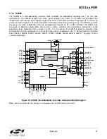
Page 174: ...Si53xx RM 174 Rev 0 52 Figure 99 Si5374 Si5375 DSPLL A ...
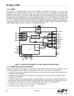
Page 175: ...Si53xx RM Rev 0 52 175 Figure 100 Si5374 Si5375 DSPLL B ...
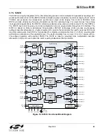
Page 176: ...Si53xx RM 176 Rev 0 52 Figure 101 Si5374 Si5375 DSPLL C ...


