


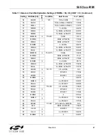


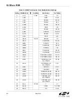

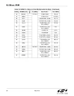

S i 5 3 x x - R M
48
Rev. 0.52
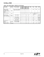
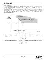
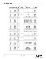
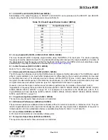
5.2.3. Jitter Tolerance
Jitter tolerance is defined as the maximum peak-to-peak sinusoidal jitter that can be present on the incoming clock
before the DSPLL loses lock. The tolerance is a function of the jitter frequency, because tolerance improves for
lower input jitter frequency.
The jitter tolerance of the DSPLL is a function of the loop bandwidth setting. Figure 23 shows the general shape of
the jitter tolerance curve versus input jitter frequency. For jitter frequencies above the loop bandwidth, the tolerance
is a constant value A
j0
. Beginning at the PLL bandwidth, the tolerance increases at a rate of 20 dB/decade for
lower input jitter frequencies.
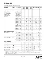
Figure 23. Jitter Tolerance Mask/Template
The equation for the high frequency jitter tolerance can be expressed as a function of the PLL loop bandwidth (i.e.,
bandwidth):
For example, the jitter tolerance when f
in
= 155.52 MHz, f
out
= 622.08 MHz and the loop bandwidth (BW) is 100 Hz:
Input
Jitter
Amplitude
A
j0
–20 dB/dec.
f
Jitter In
Excessive Input Jitter Range
BW/100 BW/10
BW
A
j0
5000
BW
-------------
ns pk-pk
=
A
j0
5000
100
-------------
50 ns pk-pk
=
=
Summary of Contents for Si5316 Series
Page 2: ...Si53xx RM 2 Rev 0 52 ...
Page 110: ...Si53xx RM 110 Rev 0 52 Figure 48 sfout_5 LVPECL Figure 49 sfout_6 CML ...
Page 111: ...Si53xx RM Rev 0 52 111 Figure 50 sfout_7 LVDS ...
Page 127: ...Si53xx RM Rev 0 52 127 Figure 66 155 52 MHz In 622 08 MHz Out Loop BW 7 Hz Si5324 ...
Page 128: ...Si53xx RM 128 Rev 0 52 Figure 67 19 44 MHz In 156 25 MHz Out Loop BW 80 Hz ...
Page 129: ...Si53xx RM Rev 0 52 129 Figure 68 19 44 MHz In 156 25 MHz Out Loop BW 5 Hz Si5324 ...
Page 131: ...Si53xx RM Rev 0 52 131 Figure 70 61 44 MHz In 491 52 MHz Out Loop BW 7 Hz Si5324 ...
Page 132: ...Si53xx RM 132 Rev 0 52 Figure 71 622 08 MHz In 672 16 MHz Out Loop BW 6 9 kHz ...
Page 133: ...Si53xx RM Rev 0 52 133 Figure 72 622 08 MHz In 672 16 MHz Out Loop BW 100 Hz ...
Page 134: ...Si53xx RM 134 Rev 0 52 Figure 73 156 25 MHz In 155 52 MHz Out ...
Page 139: ...Si53xx RM Rev 0 52 139 Figure 78 86 685 MHz In 173 371 MHz Out ...
Page 140: ...Si53xx RM 140 Rev 0 52 Figure 79 86 685 MHz In 693 493 MHz Out ...
Page 142: ...Si53xx RM 142 Rev 0 52 Figure 81 10 MHz In 1 GHz Out ...
Page 174: ...Si53xx RM 174 Rev 0 52 Figure 99 Si5374 Si5375 DSPLL A ...
Page 175: ...Si53xx RM Rev 0 52 175 Figure 100 Si5374 Si5375 DSPLL B ...
Page 176: ...Si53xx RM 176 Rev 0 52 Figure 101 Si5374 Si5375 DSPLL C ...


