


Si53xx-RM
Rev. 0.52
49
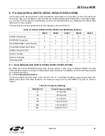
6. Pin Control Parts (Si5316, Si5322, Si5323, Si5365, Si5366)
These parts provide high-performance clock multiplication with simple pin control. Many of the control inputs are
three levels: High, Low, and Medium. High and Low are standard voltage levels determined by the supply voltage:
V
DD
and Ground. If the input pin is left floating, it is driven to nominally half of V
DD
. Effectively, this creates three
logic levels for these controls.
These parts span a range of applications and I/O capacity as shown in Table 12.
6.1. Clock Multiplication (Si5316, Si5322, Si5323, Si5365, Si5366)
By setting the tri-level FRQSEL[3:0] pins these devices provide a wide range of standard SONET and data
communications frequency scaling, including simple integer frequency multiplication to fractional settings required
for coding and decoding.
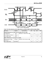
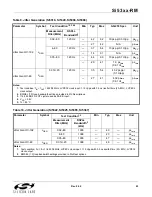
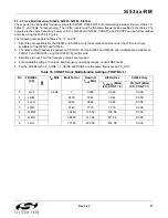
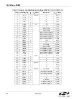
6.1.1. Clock Multiplication (Si5316)
The device accepts dual input clocks in the 19, 39, 78, 155, 311, or 622 MHz frequency range and generates a de-
jittered output clock at the same frequency. The frequency range is set by the FRQSEL [1:0] pins, as shown in
Table 13.
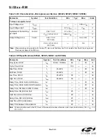
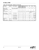
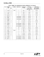
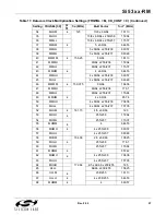
Table 12. Si5316, Si5322, Si5323, Si5365 and Si5366 Key Features
Si5316
Si5322
Si5323
Si5365
Si5366
SONET Frequencies
DATACOM Frequencies
DATACOM/SONET internetworking
Fixed Ratio between input clocks
Flexible Frequency Plan
Number of Inputs
2
2
2
4
4
Number of Outputs
1
2
2
5
5
Jitter Attenuation
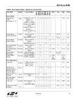
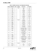
Table 13. Frequency Settings
FRQSEL[1:0]
Output Frequency (MHz)
LL
19.38–22.28
LM
38.75–44.56
LH
77.50–89.13
ML
155.00–178.25
MM
310.00–356.50
MH
620.00–710.00
Summary of Contents for Si5316 Series
Page 2: ...Si53xx RM 2 Rev 0 52 ...
Page 110: ...Si53xx RM 110 Rev 0 52 Figure 48 sfout_5 LVPECL Figure 49 sfout_6 CML ...
Page 111: ...Si53xx RM Rev 0 52 111 Figure 50 sfout_7 LVDS ...
Page 127: ...Si53xx RM Rev 0 52 127 Figure 66 155 52 MHz In 622 08 MHz Out Loop BW 7 Hz Si5324 ...
Page 128: ...Si53xx RM 128 Rev 0 52 Figure 67 19 44 MHz In 156 25 MHz Out Loop BW 80 Hz ...
Page 129: ...Si53xx RM Rev 0 52 129 Figure 68 19 44 MHz In 156 25 MHz Out Loop BW 5 Hz Si5324 ...
Page 131: ...Si53xx RM Rev 0 52 131 Figure 70 61 44 MHz In 491 52 MHz Out Loop BW 7 Hz Si5324 ...
Page 132: ...Si53xx RM 132 Rev 0 52 Figure 71 622 08 MHz In 672 16 MHz Out Loop BW 6 9 kHz ...
Page 133: ...Si53xx RM Rev 0 52 133 Figure 72 622 08 MHz In 672 16 MHz Out Loop BW 100 Hz ...
Page 134: ...Si53xx RM 134 Rev 0 52 Figure 73 156 25 MHz In 155 52 MHz Out ...
Page 139: ...Si53xx RM Rev 0 52 139 Figure 78 86 685 MHz In 173 371 MHz Out ...
Page 140: ...Si53xx RM 140 Rev 0 52 Figure 79 86 685 MHz In 693 493 MHz Out ...
Page 142: ...Si53xx RM 142 Rev 0 52 Figure 81 10 MHz In 1 GHz Out ...
Page 174: ...Si53xx RM 174 Rev 0 52 Figure 99 Si5374 Si5375 DSPLL A ...
Page 175: ...Si53xx RM Rev 0 52 175 Figure 100 Si5374 Si5375 DSPLL B ...
Page 176: ...Si53xx RM 176 Rev 0 52 Figure 101 Si5374 Si5375 DSPLL C ...