


Si53xx-RM
Rev. 0.52
51
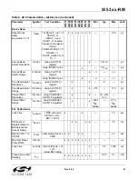
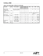
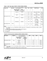
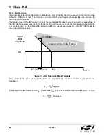
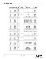
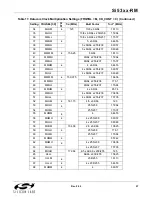
6.1.2. Clock Multiplication (Si5322, Si5323, Si5365, Si5366)
These parts provide flexible frequency plans for SONET, DATACOM, and interworking between the two (Table 16,
Table 17, and
Table 18 respectively). The CKINn inputs must be the same frequency as specified in the tables. The
outputs are the same frequency; however, in the Si5365 and Si5366, CKOUT3 and CKOUT4 can be further divided
down by using the DIV34 [1:0] pins.
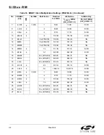
The following notes apply to Tables 16, 17, and 18:
1. All entries are available for the Si5323 and Si5366. Only those marked entries under the WB column are
available for the Si5322 and Si5365.
2. The listed output frequencies appear on CKOUTn. For the Si5365 and Si5366, sub-multiples are available on
CKOUT3 and CKOUT4 using the DIV34[1:0] control pins.
3. All ratios are exact, but the frequency values are rounded.
4. For bandwidth settings, f3 values, and frequency operating ranges, consult DSPLL
sim
.
5. For the Si5366 with CK_CONF = 1, CKIN3 and CKIN4 are the same frequency as FS_OUT.
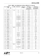
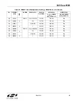
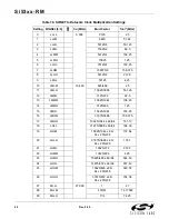
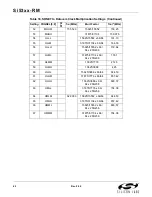
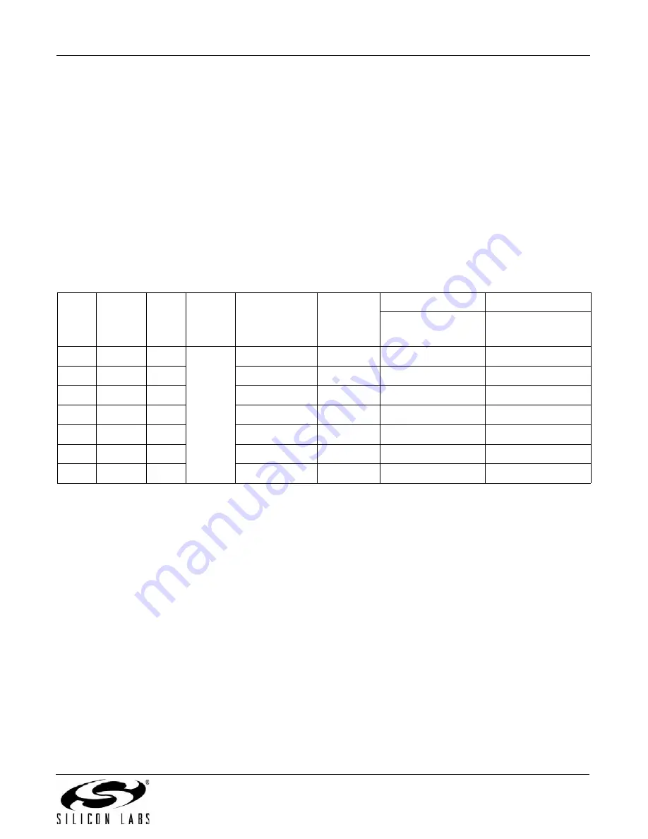
Table 16. SONET Clock Multiplication Settings (FRQTBL=L)
No
FRQSEL
[3:0]
WB
f
IN
MHz
Mult Factor
Nominal
f
OUT
MHz
All Devices
Si5366 Only
f
CKOUT5
(MHz)
(CK_CONF = 0)
FS_OUT (MHz)
(CK_CONF = 1)
0
LLLL
0.008
1
0.008
0.008
0.008
1
LLLM
2430
19.44
19.44
0.008
2
LLLH
4860
38.88
38.88
0.008
3
LLML
9720
77.76
77.76
0.008
4
LLMM
19440
155.52
155.52
0.008
5
LLMH
38880
311.04
311.04
0.008
6
LLHL
77760
622.08
622.08
0.008
Summary of Contents for Si5316 Series
Page 2: ...Si53xx RM 2 Rev 0 52 ...
Page 110: ...Si53xx RM 110 Rev 0 52 Figure 48 sfout_5 LVPECL Figure 49 sfout_6 CML ...
Page 111: ...Si53xx RM Rev 0 52 111 Figure 50 sfout_7 LVDS ...
Page 127: ...Si53xx RM Rev 0 52 127 Figure 66 155 52 MHz In 622 08 MHz Out Loop BW 7 Hz Si5324 ...
Page 128: ...Si53xx RM 128 Rev 0 52 Figure 67 19 44 MHz In 156 25 MHz Out Loop BW 80 Hz ...
Page 129: ...Si53xx RM Rev 0 52 129 Figure 68 19 44 MHz In 156 25 MHz Out Loop BW 5 Hz Si5324 ...
Page 131: ...Si53xx RM Rev 0 52 131 Figure 70 61 44 MHz In 491 52 MHz Out Loop BW 7 Hz Si5324 ...
Page 132: ...Si53xx RM 132 Rev 0 52 Figure 71 622 08 MHz In 672 16 MHz Out Loop BW 6 9 kHz ...
Page 133: ...Si53xx RM Rev 0 52 133 Figure 72 622 08 MHz In 672 16 MHz Out Loop BW 100 Hz ...
Page 134: ...Si53xx RM 134 Rev 0 52 Figure 73 156 25 MHz In 155 52 MHz Out ...
Page 139: ...Si53xx RM Rev 0 52 139 Figure 78 86 685 MHz In 173 371 MHz Out ...
Page 140: ...Si53xx RM 140 Rev 0 52 Figure 79 86 685 MHz In 693 493 MHz Out ...
Page 142: ...Si53xx RM 142 Rev 0 52 Figure 81 10 MHz In 1 GHz Out ...
Page 174: ...Si53xx RM 174 Rev 0 52 Figure 99 Si5374 Si5375 DSPLL A ...
Page 175: ...Si53xx RM Rev 0 52 175 Figure 100 Si5374 Si5375 DSPLL B ...
Page 176: ...Si53xx RM 176 Rev 0 52 Figure 101 Si5374 Si5375 DSPLL C ...