


S i 5 3 x x - R M
68
Rev. 0.52
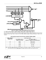
At power-on or reset, the valid CKINn with the highest priority (1 being the highest priority) is automatically
selected. If no valid CKINn is available, the device suppresses the output clocks and waits for a valid CKINn signal.
If the currently selected CKINn goes into an alarm state, the next valid CKINn in priority order is selected. If no valid
CKINn is available, the device enters Digital Hold.
Operation in revertive and non- revertive is different when a signal becomes valid:
Revertive (AUTOSEL = H):
The device constantly monitors all CKINn. If a CKINn with a higher priority than
the current active CKINn becomes valid, the active CKINn is changed to the
CKINn with the highest priority.
Non-revertive (AUTOSEL = M): The active clock does not change until there is an alarm on the active clock. The
device will then select the highest priority CKINn that is valid. Once in digital hold,
the device will switch to the first CKINn that becomes valid.
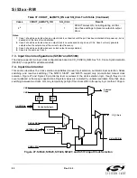
6.3.3. Hitless Switching with Phase Build-Out (Si5323, Si5366)
Silicon Laboratories switching technology performs “phase build-out” to minimize the propagation of phase
transients to the clock outputs during input clock switching. All switching between input clocks occurs within the
input multiplexor and phase detector circuitry. The phase detector circuitry continually monitors the phase
difference between each input clock and the DSPLL output clock, f
OSC
. The phase detector circuitry can lock to a
clock signal at a specified phase offset relative to f
OSC
so that the phase offset is maintained by the PLL circuitry.
At the time a clock switch occurs, the phase detector circuitry knows both the input-to-output phase relationship for
the original input clock and for the new input clock. The phase detector circuitry locks to the new input clock at the
new clock's phase offset so that the phase of the output clock is not disturbed. The phase difference between the
two input clocks is absorbed in the phase detector's offset value, rather than being propagated to the clock output.
The switching technology virtually eliminates the output clock phase transients traditionally associated with clock
rearrangement (input clock switching).
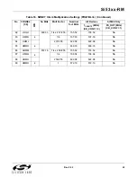
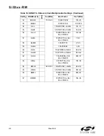
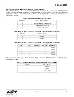
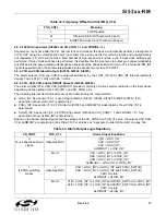
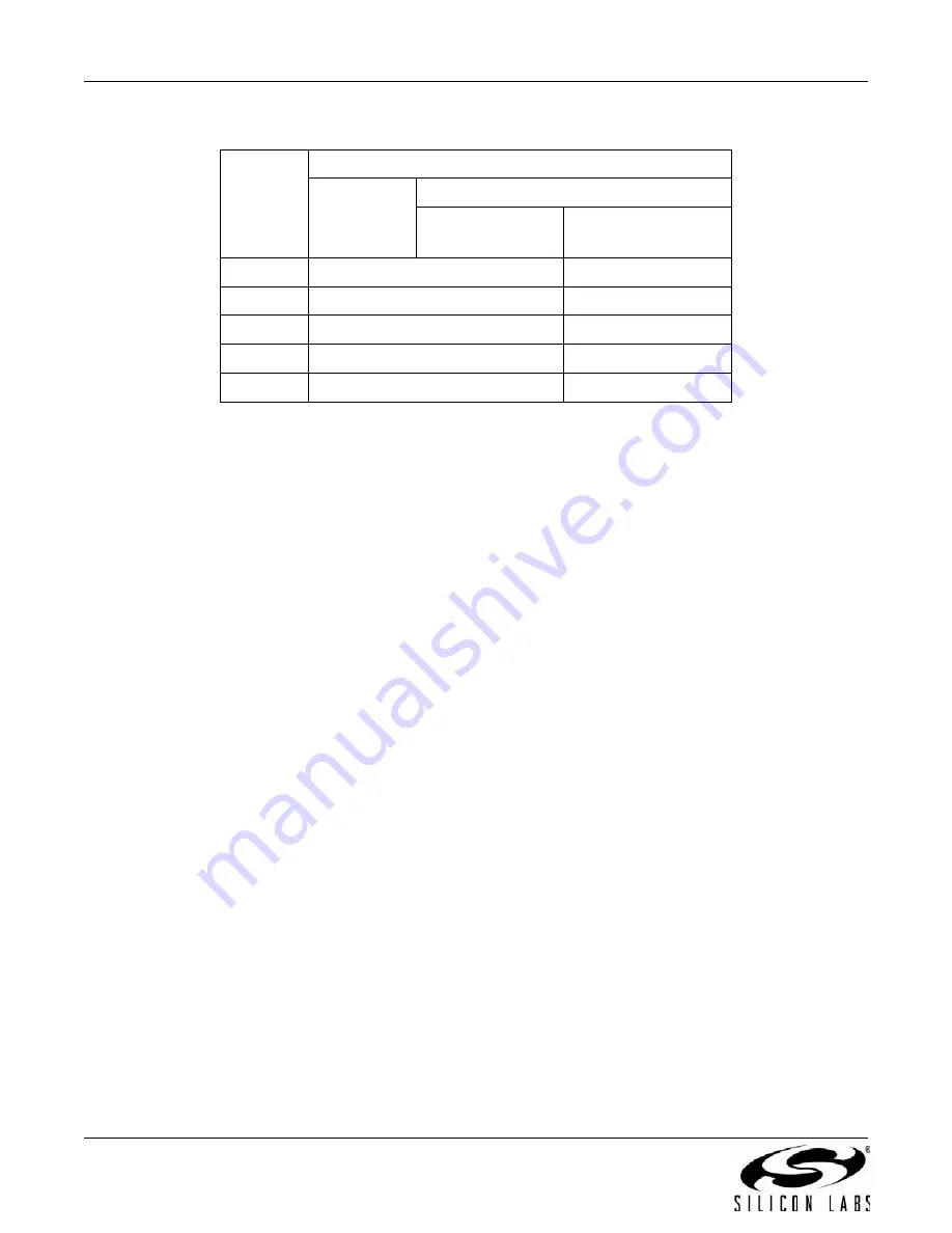
Table 28. Input Clock Priority for Auto Switching (Si5365, Si5366)
Priority
Input Clock Configuration
Si5365
Si5366
4 Input Clocks
(CK_CONF = 0)
FSYNC Switching
(CK_CONF = 1)
1
CKIN1
CKIN1/CKIN3
2
CKIN2
CKIN2/CKIN4
3
CKIN3
N/A
4
CKIN4
N/A
5
Digital Hold
Digital Hold
Summary of Contents for Si5316 Series
Page 2: ...Si53xx RM 2 Rev 0 52 ...
Page 110: ...Si53xx RM 110 Rev 0 52 Figure 48 sfout_5 LVPECL Figure 49 sfout_6 CML ...
Page 111: ...Si53xx RM Rev 0 52 111 Figure 50 sfout_7 LVDS ...
Page 127: ...Si53xx RM Rev 0 52 127 Figure 66 155 52 MHz In 622 08 MHz Out Loop BW 7 Hz Si5324 ...
Page 128: ...Si53xx RM 128 Rev 0 52 Figure 67 19 44 MHz In 156 25 MHz Out Loop BW 80 Hz ...
Page 129: ...Si53xx RM Rev 0 52 129 Figure 68 19 44 MHz In 156 25 MHz Out Loop BW 5 Hz Si5324 ...
Page 131: ...Si53xx RM Rev 0 52 131 Figure 70 61 44 MHz In 491 52 MHz Out Loop BW 7 Hz Si5324 ...
Page 132: ...Si53xx RM 132 Rev 0 52 Figure 71 622 08 MHz In 672 16 MHz Out Loop BW 6 9 kHz ...
Page 133: ...Si53xx RM Rev 0 52 133 Figure 72 622 08 MHz In 672 16 MHz Out Loop BW 100 Hz ...
Page 134: ...Si53xx RM 134 Rev 0 52 Figure 73 156 25 MHz In 155 52 MHz Out ...
Page 139: ...Si53xx RM Rev 0 52 139 Figure 78 86 685 MHz In 173 371 MHz Out ...
Page 140: ...Si53xx RM 140 Rev 0 52 Figure 79 86 685 MHz In 693 493 MHz Out ...
Page 142: ...Si53xx RM 142 Rev 0 52 Figure 81 10 MHz In 1 GHz Out ...
Page 174: ...Si53xx RM 174 Rev 0 52 Figure 99 Si5374 Si5375 DSPLL A ...
Page 175: ...Si53xx RM Rev 0 52 175 Figure 100 Si5374 Si5375 DSPLL B ...
Page 176: ...Si53xx RM 176 Rev 0 52 Figure 101 Si5374 Si5375 DSPLL C ...


