


Si53xx-RM
Rev. 0.52
77
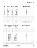
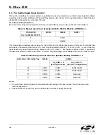
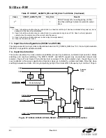
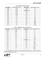
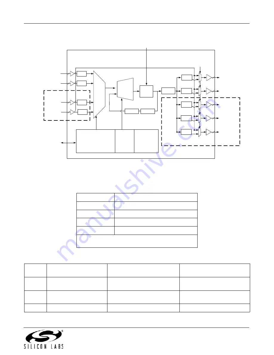
Figure 26. Narrowband PLL Divider Settings
(Si5319, Si5324, Si5326, Si5327, Si5368, Si5369, Si5374, Si5375)
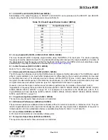
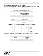
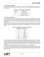
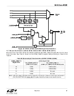
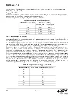
Table 35. Narrowband Frequency Limits
Signal
Frequency Limits
CKINn
2 kHz–710 MHz
f
3
2 kHz–2 MHz
f
OSC
4.85–5.67 GHz
f
OUT
2 kHz–1.475 GHz
Note:
Fmax = 808 MHz for the Si5327, Si5374 and Si5375. Each
entry has 500 ppm margins at both ends.
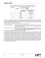
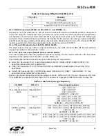
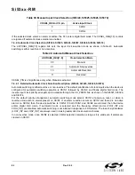
Table 36. Dividers and Limits
Divider
Equation
Si5325, Si5367
Si5319, Si5324, Si5326, Si5327,
Si5368, Si5369, Si5374, Si5375
N1
N1 = N1_HS x NCn_LS
N1_HS = [4, 5, …, 11]
NCn_LS = [1, 2, 4, 6, …, 2^20]
N1_HS = [4, 5, …, 11]
NCn_LS = [1, 2, 4, 6, …, 2^20]
N2
N2 = N2_HS x N2_LS
N2_HS = 1
N2_LS = [32, 34, 36, …, 2^9]
N2_HS = [4, 5, …, 11]
N2_LS = [2, 4, 6, …, 2^20]
N3
N3 = N3n
N3n = [1,2,3,..,2^19]
N3n = [1,2,3,..,2^19]
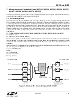
CKIN_1–
CKIN_2–
CKIN_3–
CKIN_4–
CKOUT_1–
÷ NC1
1
0
CKOUT_2–
÷ NC2
1
0
CKOUT_3–
÷ NC3
1
0
CKOUT_4–
÷ NC4
1
0
2
2
2
2
2
2
2
2
DCO
f
OSC
Xtal, or Refclock
(
Si5319, Si5324, Si5326, Si5327, Si5368, Si5369;
Refclock only for the Si5374 and Si5375
)
f
x
M
f
3
Digital
Phase
Detector/
Loop Filter
BYPASS
f
3
SPI/I
2
C
Si5319, Si5326,
Si5368
Control
÷ N32
÷ N31
Si5368
Si5368
Note: See section 6.7
for FSYNC details.
÷ N1_HS
CKOUT_5–
÷ NC5
1
0
2
÷ N33
÷ N34
Note: There are multiple outputs at different frequencies because of limitations caused by the DCO and N1_HS.
÷ N2_LS
÷ N2_HS
Bandwidth
Control
FSYNC
(Si5368)
Si5369
Si5369
Summary of Contents for Si5316 Series
Page 2: ...Si53xx RM 2 Rev 0 52 ...
Page 110: ...Si53xx RM 110 Rev 0 52 Figure 48 sfout_5 LVPECL Figure 49 sfout_6 CML ...
Page 111: ...Si53xx RM Rev 0 52 111 Figure 50 sfout_7 LVDS ...
Page 127: ...Si53xx RM Rev 0 52 127 Figure 66 155 52 MHz In 622 08 MHz Out Loop BW 7 Hz Si5324 ...
Page 128: ...Si53xx RM 128 Rev 0 52 Figure 67 19 44 MHz In 156 25 MHz Out Loop BW 80 Hz ...
Page 129: ...Si53xx RM Rev 0 52 129 Figure 68 19 44 MHz In 156 25 MHz Out Loop BW 5 Hz Si5324 ...
Page 131: ...Si53xx RM Rev 0 52 131 Figure 70 61 44 MHz In 491 52 MHz Out Loop BW 7 Hz Si5324 ...
Page 132: ...Si53xx RM 132 Rev 0 52 Figure 71 622 08 MHz In 672 16 MHz Out Loop BW 6 9 kHz ...
Page 133: ...Si53xx RM Rev 0 52 133 Figure 72 622 08 MHz In 672 16 MHz Out Loop BW 100 Hz ...
Page 134: ...Si53xx RM 134 Rev 0 52 Figure 73 156 25 MHz In 155 52 MHz Out ...
Page 139: ...Si53xx RM Rev 0 52 139 Figure 78 86 685 MHz In 173 371 MHz Out ...
Page 140: ...Si53xx RM 140 Rev 0 52 Figure 79 86 685 MHz In 693 493 MHz Out ...
Page 142: ...Si53xx RM 142 Rev 0 52 Figure 81 10 MHz In 1 GHz Out ...
Page 174: ...Si53xx RM 174 Rev 0 52 Figure 99 Si5374 Si5375 DSPLL A ...
Page 175: ...Si53xx RM Rev 0 52 175 Figure 100 Si5374 Si5375 DSPLL B ...
Page 176: ...Si53xx RM 176 Rev 0 52 Figure 101 Si5374 Si5375 DSPLL C ...