


Si53xx-RM
Rev. 0.52
81
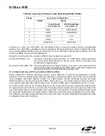
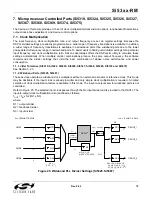
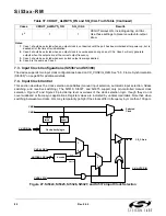
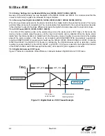
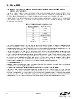
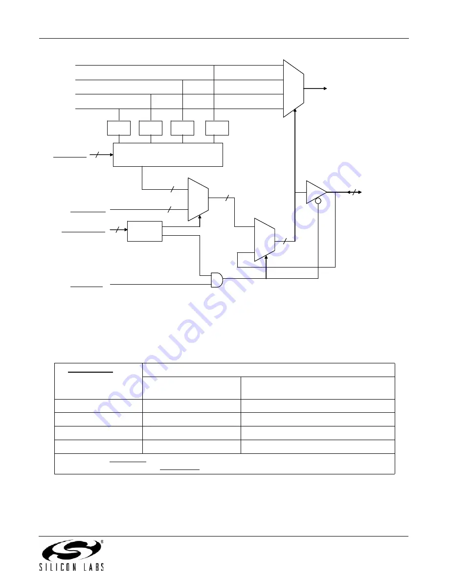
Figure 28. Si5367, Si5368, and Si5369 Input Clock Selection
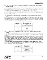
7.4.1. Manual Clock Selection (Si5324, Si5325, Si5326, Si5367, Si5368, Si5369, Si5374)
Manual control of input clock selection is available by setting the
AUTOSEL_REG
[1:0] register bits to 00. In manual
mode, the active input clock is chosen via the
CKSEL_REG
[1:0] register setting according to Table 38 and
Table 39.
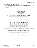
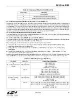
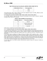
Table 38. Manual Input Clock Selection (Si5367, Si5368, Si5369)
CKSEL_REG[1:0]
Register Bits
Active Input Clock
CK_CONFIG_REG = 0
(CKIN1,2,3,4 inputs)
CK_CONFIG_REG = 1
(CKIN1,3 & CKIN2,4 clock/FSYNC pairs)
00
CKIN1
CKIN1/CKIN3
01
CKIN2
CKIN2/CKIN4
10
CKIN3
Not used
11
CKIN4
Not used
Note:
Setting the
CKSEL_PIN
register bit to one allows the CS [1:0] pins to continue to control input clock selection.
If CS_PIN is set to zero, the
CKSEL_REG
[1:0] register bits perform the input clock selection function.
CKIN1
CKIN2
CKIN3
CKIN4
Clock priority logic
CK_PRIORn
0
1
CKSEL_REG
AUTOSEL_REG
0
1
CKSEL_PIN
LOS/FOS
detect
LOS/FOS
detect
LOS/FOS
detect
LOS/FOS
detect
decode
Auto
Manual
Selected
Clock
2
2
2
2
2
8
2
CS0_C3A,
CS1_C4A
pins
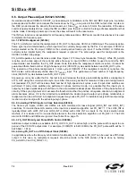
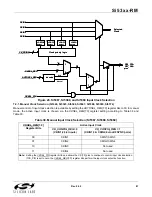
CKIN1
CKIN2
CKIN3
CKIN4
Clock priority logic
CK_PRIORn
0
1
CKSEL_REG
AUTOSEL_REG
0
1
CKSEL_PIN
LOS/FOS
detect
LOS/FOS
detect
LOS/FOS
detect
LOS/FOS
detect
LOS/FOS
detect
LOS/FOS
detect
LOS/FOS
detect
LOS/FOS
detect
decode
Auto
Manual
Selected
Clock
2
2
2
2
2
8
2
CS0_C3A,
CS1_C4A
pins
Summary of Contents for Si5316 Series
Page 2: ...Si53xx RM 2 Rev 0 52 ...
Page 110: ...Si53xx RM 110 Rev 0 52 Figure 48 sfout_5 LVPECL Figure 49 sfout_6 CML ...
Page 111: ...Si53xx RM Rev 0 52 111 Figure 50 sfout_7 LVDS ...
Page 127: ...Si53xx RM Rev 0 52 127 Figure 66 155 52 MHz In 622 08 MHz Out Loop BW 7 Hz Si5324 ...
Page 128: ...Si53xx RM 128 Rev 0 52 Figure 67 19 44 MHz In 156 25 MHz Out Loop BW 80 Hz ...
Page 129: ...Si53xx RM Rev 0 52 129 Figure 68 19 44 MHz In 156 25 MHz Out Loop BW 5 Hz Si5324 ...
Page 131: ...Si53xx RM Rev 0 52 131 Figure 70 61 44 MHz In 491 52 MHz Out Loop BW 7 Hz Si5324 ...
Page 132: ...Si53xx RM 132 Rev 0 52 Figure 71 622 08 MHz In 672 16 MHz Out Loop BW 6 9 kHz ...
Page 133: ...Si53xx RM Rev 0 52 133 Figure 72 622 08 MHz In 672 16 MHz Out Loop BW 100 Hz ...
Page 134: ...Si53xx RM 134 Rev 0 52 Figure 73 156 25 MHz In 155 52 MHz Out ...
Page 139: ...Si53xx RM Rev 0 52 139 Figure 78 86 685 MHz In 173 371 MHz Out ...
Page 140: ...Si53xx RM 140 Rev 0 52 Figure 79 86 685 MHz In 693 493 MHz Out ...
Page 142: ...Si53xx RM 142 Rev 0 52 Figure 81 10 MHz In 1 GHz Out ...
Page 174: ...Si53xx RM 174 Rev 0 52 Figure 99 Si5374 Si5375 DSPLL A ...
Page 175: ...Si53xx RM Rev 0 52 175 Figure 100 Si5374 Si5375 DSPLL B ...
Page 176: ...Si53xx RM 176 Rev 0 52 Figure 101 Si5374 Si5375 DSPLL C ...