
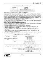


S i 5 3 x x - R M
86
Rev. 0.52
7.6. Digital Hold
All Any-Frequency Precision Clock devices feature a holdover mode, whereby the DSPLL is locked to a digital
value.
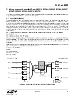
7.6.1. Narrowband Digital Hold (Si5316, Si5324, Si5326, Si5368, Si5369, Si5374)
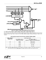
After the part's initial self-calibration (ICAL), when no valid input clock is available, the device enters digital hold.
Referring to the logical diagram in "Appendix D—Alarm Structure" on page 144, lack of clock availability is defined
by following the boolean equation for the Si5324, Si5326, and Si5374:
(LOS1_INT OR FOS1_INT) AND (LOS2_INT OR FOS2_INT) = enter digital hold
The equivalent Boolean equation for the Si5327 is as follows:
LOS1 and LOS2 = enter digital hold
The equivalent boolean equation for the Si5367, Si5368, and Si5369 is as follows:
(LOS1_INT OR FOS1_INT) AND (LOS2_INT OR FOS2_INT) AND
(LOS3_INT OR FOS3_INT) AND (LOS4_INT OR FOS4_INT) = enter digital hold
7.6.1.1. Digital Hold Detailed Description (Si5324, Si5326, Si5327, Si5368, Si5369, Si5374)
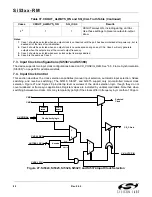
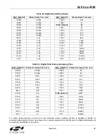
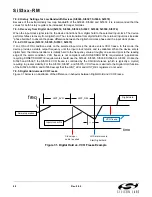
In this mode, the device provides a stable output frequency until the input clock returns and is validated. Upon
entering digital hold, the internal DCO is initially held to its last frequency value, M (See Figure 30). Next, the DCO
slowly transitions to a historical average frequency value supplied to the DSPLL, M
HIST
, as shown in Figure 30.
Values of M starting from time t = –(
HIST_DEL
+
HIST_AVG
) and ending at t = –
HIST_DEL
are averaged to
compute M
HIST
. This historical average frequency value is taken from an internal memory location that keeps a
record of previous M values supplied to the DCO. By using a historical average frequency, input clock phase and
frequency transients that may occur immediately preceding digital hold do not affect the digital hold frequency.
Also, noise related to input clock jitter or internal PLL jitter is minimized.
Figure 30. Parameters in History Value of M
The history delay can be set via the
HIST_DEL
[4:0] register bits as shown in Table 42 and the history averaging
time can be set via the
HIST_AVG
[4:0] register bits as shown in Table 43. The
DIGHOLDVALID
register can be
used to determine if the information in
HIST_AVG
is valid and the device can enter SONET/SDH compliant digital
hold. If
DIGHOLDVALID
is not active, the part will enter VCO freeze instead of digital hold.
Time
Digital Hold
@
t = 0
M
M
HIST
t = –
HIST_DEL
HIST_AVG
Summary of Contents for Si5316 Series
Page 2: ...Si53xx RM 2 Rev 0 52 ...
Page 110: ...Si53xx RM 110 Rev 0 52 Figure 48 sfout_5 LVPECL Figure 49 sfout_6 CML ...
Page 111: ...Si53xx RM Rev 0 52 111 Figure 50 sfout_7 LVDS ...
Page 127: ...Si53xx RM Rev 0 52 127 Figure 66 155 52 MHz In 622 08 MHz Out Loop BW 7 Hz Si5324 ...
Page 128: ...Si53xx RM 128 Rev 0 52 Figure 67 19 44 MHz In 156 25 MHz Out Loop BW 80 Hz ...
Page 129: ...Si53xx RM Rev 0 52 129 Figure 68 19 44 MHz In 156 25 MHz Out Loop BW 5 Hz Si5324 ...
Page 131: ...Si53xx RM Rev 0 52 131 Figure 70 61 44 MHz In 491 52 MHz Out Loop BW 7 Hz Si5324 ...
Page 132: ...Si53xx RM 132 Rev 0 52 Figure 71 622 08 MHz In 672 16 MHz Out Loop BW 6 9 kHz ...
Page 133: ...Si53xx RM Rev 0 52 133 Figure 72 622 08 MHz In 672 16 MHz Out Loop BW 100 Hz ...
Page 134: ...Si53xx RM 134 Rev 0 52 Figure 73 156 25 MHz In 155 52 MHz Out ...
Page 139: ...Si53xx RM Rev 0 52 139 Figure 78 86 685 MHz In 173 371 MHz Out ...
Page 140: ...Si53xx RM 140 Rev 0 52 Figure 79 86 685 MHz In 693 493 MHz Out ...
Page 142: ...Si53xx RM 142 Rev 0 52 Figure 81 10 MHz In 1 GHz Out ...
Page 174: ...Si53xx RM 174 Rev 0 52 Figure 99 Si5374 Si5375 DSPLL A ...
Page 175: ...Si53xx RM Rev 0 52 175 Figure 100 Si5374 Si5375 DSPLL B ...
Page 176: ...Si53xx RM 176 Rev 0 52 Figure 101 Si5374 Si5375 DSPLL C ...


