


Si53xx-RM
Rev. 0.52
97
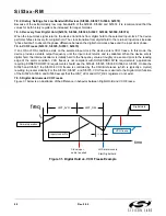
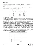
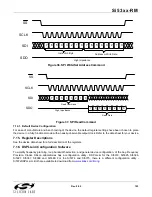
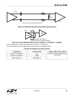
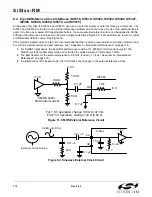
Both the FOS reference and the FOS monitored clock must be divided down to the same clock rate and this clock
rate must be between 10 MHz and 27 MHz. As can be seen in Figure 33, the values for P and Q must be selected
so that the FOS comparison occurs at the same frequency. The registers that contain the values for P and Q are
the
CKINnRATE[2:0]
registers.
Figure 33. FOS Compare
The frequency band of each input clock must be specified to use the FOS feature. The
CLKNRATE
registers
specify the frequency of the device input clocks as shown in Table 51.
When the FOS reference is the XA/XB oscillator (either internal or external), the value of Q in Figure 33 is always
2, for an effective
CLKINnRATE
of 1, as shown in Table 51.
For example, to monitor a 544 MHz clock at CKIN1 with a FOS reference of 34 MHz at CKIN2:
CLK1RATE = 5
CLK2RATE = 1
FOSREFSEL[2:0] = 010
Table 50. FOS Reference Clock Selection
FOS Reference
FOSREFSEL[2:0]
Si5326
Si5368
000
XA/XB
XA/XB
001
CKIN1
CKIN1
010
CKIN2 (default)
CKIN2 (default)
011
Reserved
CKIN3
100
Reserved
CKIN4
all others
Reserved
Reserved
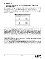
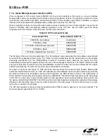
Table 51. CLKnRATE Registers
CLKnRATE
Divisor, P or Q
Min Frequency, MHz
Max Frequency, MHz
0
1
10
27
1
2
25
54
2
4
50
105
3
8
95
215
4
16
190
435
5
32
375
710
CKIN
FOS_REF
P
Q
FOS
Compare
10 MHz min,
27 MHz max
Summary of Contents for Si5316 Series
Page 2: ...Si53xx RM 2 Rev 0 52 ...
Page 110: ...Si53xx RM 110 Rev 0 52 Figure 48 sfout_5 LVPECL Figure 49 sfout_6 CML ...
Page 111: ...Si53xx RM Rev 0 52 111 Figure 50 sfout_7 LVDS ...
Page 127: ...Si53xx RM Rev 0 52 127 Figure 66 155 52 MHz In 622 08 MHz Out Loop BW 7 Hz Si5324 ...
Page 128: ...Si53xx RM 128 Rev 0 52 Figure 67 19 44 MHz In 156 25 MHz Out Loop BW 80 Hz ...
Page 129: ...Si53xx RM Rev 0 52 129 Figure 68 19 44 MHz In 156 25 MHz Out Loop BW 5 Hz Si5324 ...
Page 131: ...Si53xx RM Rev 0 52 131 Figure 70 61 44 MHz In 491 52 MHz Out Loop BW 7 Hz Si5324 ...
Page 132: ...Si53xx RM 132 Rev 0 52 Figure 71 622 08 MHz In 672 16 MHz Out Loop BW 6 9 kHz ...
Page 133: ...Si53xx RM Rev 0 52 133 Figure 72 622 08 MHz In 672 16 MHz Out Loop BW 100 Hz ...
Page 134: ...Si53xx RM 134 Rev 0 52 Figure 73 156 25 MHz In 155 52 MHz Out ...
Page 139: ...Si53xx RM Rev 0 52 139 Figure 78 86 685 MHz In 173 371 MHz Out ...
Page 140: ...Si53xx RM 140 Rev 0 52 Figure 79 86 685 MHz In 693 493 MHz Out ...
Page 142: ...Si53xx RM 142 Rev 0 52 Figure 81 10 MHz In 1 GHz Out ...
Page 174: ...Si53xx RM 174 Rev 0 52 Figure 99 Si5374 Si5375 DSPLL A ...
Page 175: ...Si53xx RM Rev 0 52 175 Figure 100 Si5374 Si5375 DSPLL B ...
Page 176: ...Si53xx RM 176 Rev 0 52 Figure 101 Si5374 Si5375 DSPLL C ...


