Smart Machine Smart Decision
SIM868_Series_Hardware_Design_V1.06
57
2017-07-13
7.2.
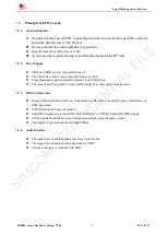
Principle of PCB Layout
7.2.1.
Antenna Interface
Antenna interface used for RF conducting test such as coaxial cable pad, RF connector
should be placed close to RF_IN pad.
RF
trace should be as short and direct as possible.
Keep the impedance of
RF traces as 50Ω;
Avoid any other signal crossing or parallel directly under the RF trace.
7.2.2.
Power Supply
VBAT and GND are very important in layout.
The VBAT trace should be as short and wide as possible.
Zener diode and capacitor should be placed close to VBAT pin.
The trace of pin 36 and pin37 to main GND should be as short and wide as possible.
7.2.3.
SIM Card Interface
Ensure SIM card holder is far away from antenna or RF cable to avoid high power interference of
GSM transmitter.
Put SIM card holder near the module.
Add ESD component to protect SIM_CLK, SIM_DATA, SIM_RST and SIM_VDD signals.
All the signals should be far away from power and high-speed-frequency signal.
The length of signals should be less than 100mm.
7.2.4.
Audio Interface
The signal trace of audio should be far away from antenna
The signal trace of audio should not parallel to VBAT
The audio trace are surrounded with GND
SIMCOM
CONFIDENTIAL
FILE


