SiRFatlasV
Hardware Design Guide
January, 2010
SiRF Design Guide
– Proprietary and Confidential
9
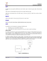
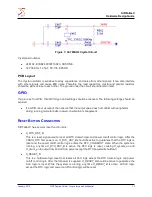
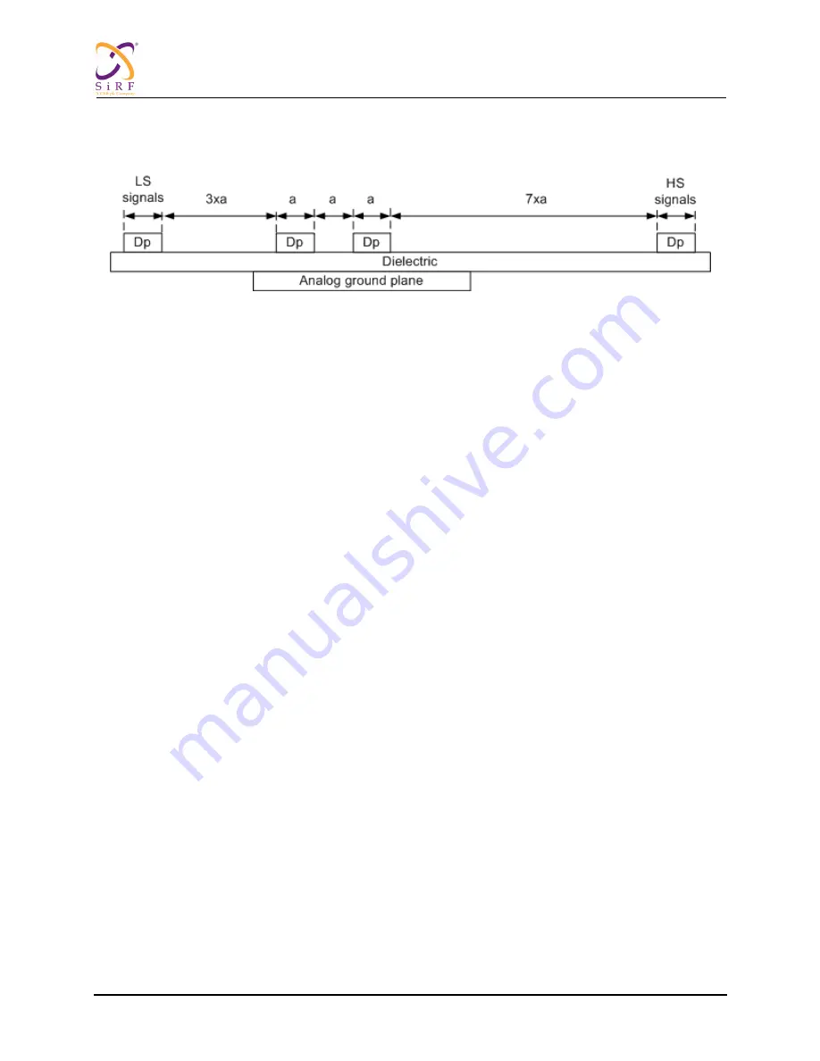
In order to minimize crosstalk, make sure that signal traces are routed close to the two USB differential
signals. The minimum recommended spacing is 3xa for low-speed non-periodic signals, and 7xa for
high-speed periodic signals. A continuous ground plane below the DP/DN lines is required.
Figure 3: USB Layout Rule
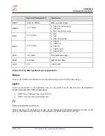
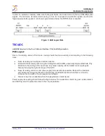
TSC/ADC
Add ESD devices to the Touch Screen Interface (TSI) for ESD protection.
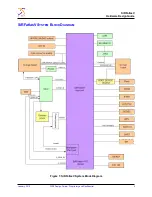
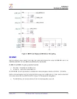
PCB Layout
Due to the analog nature of this block, routing should be done carefully and according to the following
rules:
Keep all analog net routing as small as possible.
Shield all critical analog nets using the Analog Ground (AGND), especially single-ended nets. Pay
attention to the routing of the input lines. Any noise coupling will be treated as an input signal,
thereby reducing the dynamic range of the ADC.
Keep all analog, reference and power supply lines as wide as possible. Respect the maximum
wire resistance values mentioned in the Routing Constraints section when there is a need to
increase the line width or to use several metal layers.
Use as many vias as possible when changing between metal layers.
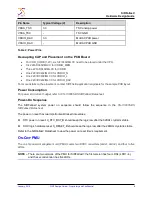
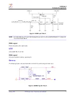
Power supply decoupling should follow the figure below. The capacitors should be good quality ceramic
and that they must be placed as close to the chip as possible.