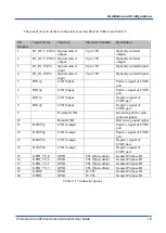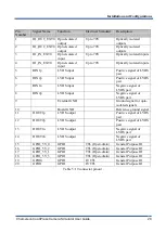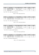
Chameleon CoaXPress Camera Simulator User Guide
21
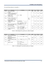
Electrical characteristics for board IO’s:
Symbol
Parameter
Condition
Pin
MIN
Typ
MAX
Units
| V
OD
|
Differential Output
Voltage
R
L
= 100 Ω
D
OUT-
D
OUT+
250
350
450
mV
∆V
OD
Change in Magnitude of
V
OD
for Complementary
Output States
1
35
| mV |
V
OS
Offset Voltage
1.12
5
1.23
1.375
V
∆V
OS
Change in Magnitude of
V
OS
for Complementary
Output States
1
25
| mV |
I
OS
Output Short Circuit
Current
(4)
ENABLED,
D
IN
= V
DD
, D
OUT+
= 0 V or
D
IN
= GND, D
OUT-
= 0 V
-5.8
-9.0
mA
I
OSD
Differential Output Short
Circuit Current
(4)
ENABLED, V
OD
= 0 V
-5.8
-9.0
mA
I
OFF
Power-off Leakage
V
OUT
= 0 V or 3.6 V
V
DD
= 0 V or Open
-20
±1
+20
µA
I
OZ
Output TRI-STATE
Current
EN = 0 V and EN = V
DD
V
OUT
= 0 V or V
DD
-10
±1
+10
µA
Table 6: LVDS Output DC specifications (Driver Outputs)
Symbol
Parameter
Condition
Pin
MIN
Typ
MAX
Units
V
TH
Differential Input High
Threshold
V
CM
= 1.2 V, 0.05 V, 2.35 V
R
IN+
R
IN
-
-15
35
mV
V
TL
Differential Input Low
Threshold
-100
-15
mV
V
CMR
Common-Mode Voltage
Range
V
ID
= 100 mV, V
DD
= 3.3 V
0.05
3
V
I
IN
Input Current
V
DD
= 3.6 V
V
IN
= 0 V or 2.8 V
-12
±4
+12
µA
V
DD
= 0 V
V
IN
= 0 V or 2.8 V or 3.6 V
-10
±1
+10
µA
Table 7: LVDS Input DC specifications (Receiver Inputs)
Installation and Configurations

