CLKIN_x
CLKIN_x#
Clock IC
External oscillator/clock source
Input buffer
100 ohms
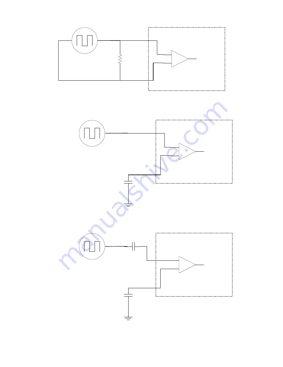
Figure 3.6. Termination for DC-Coupling an External LVDS Clock Input to CLKIN_x/CLKIN_x# Pins
CLKIN_x
CLKIN_x#
Clock IC
External oscillator/clock source
Input buffer
0.1 µF
The swing of the
clock source
should match the
VDD CORE value
Figure 3.7. Termination for DC-Coupling a Single-Ended Clock Input to CLKIN_x/CLKIN_x# Pins
CLKIN_x
CLKIN_x#
Clock IC
External oscillator/clock source
Input buffer
0.1 µF
The swing of the
clock source can
be any value
between 1V – 4V
0.1 µF
Figure 3.8. Termination for AC-Coupling a Single-Ended Clock Input to CLKIN_x/CLKIN_x# Pins
Si5357 Reference Manual • Input Clocks
Skyworks Solutions, Inc. • Phone [781] 376-3000 • Fax [781] 376-3100 • sales@skyworksinc.com • www.skyworksinc.com
8
Rev. 0.2 • Skyworks Proprietary Information • Products and Product Information are Subject to Change Without Notice • July 26, 2021
8


