5
5
4
4
3
3
2
2
1
1
D
D
C
C
B
B
A
A
FLASH_CS0N
FLASH_WP0N
SPI_Flash-SDI
SPI_Flash-SDO
SPI_Flash-SCK
RXO0+
RXO0-
R6_RXO0-
RXO1+
RXO1-
R4_RXO1-
RXO2-
R2_RXO2-
RXO2+
RXO3-
G6_RXO3-
RXO3+
RXOC-
R0_RXOC-
RXOC+
RXO4-
G4_RXO4-
RXO4+
RXE0-
G2_RXE0-
RXE0+
RXE1-
G0_RXE1-
RXE1+
RXE2-
B6_RXE2-
RXE2+
RXE3-
B2_RXE3-
RXE3+
RXEC-
B4_RXEC-
RXEC+
RXE4-
B0_RXE4-
RXE4+
SPI_WP0N
SPI_CS0N
AMP-AUOUTR0
AMP-AUOUTL0
AV_AUOUTL3
AV_AUOUTR3
AV-AUOUTR3
AV-AUOUTL3
AVSS_PGA
XTALO
XTALI
TUNER_SDA
TUNER_SCL
System-RST
AUBCK_OUT
AUMCK_OUT
CFG-PWM1
BRI_ADJ-PWM0
UART-TX
UART-RX
A-MVREF
LED_R
IRIN
IR-in
KEY0-in
KEY1-in
KEY0-SAR0
KEY1-SAR1
KEY0-in
IR-in
KEY1-in
LED
LED_G
KEY0-in
KEY1-in
IR-in
LED_GLED_G
IRIN
HDMI-CEC
System-RST
HDMI1-CLKN
HDMI1-CLKP
HDMI1-SCL
HDMI1-RX1N
HDMI1-RX1P
HDMI1-RX2N
HDMI1-RX2P
HDMI1-RX0N
HDMI1-RX0P
HDMI1-SDA
HDMI_HP1
ARC
RGB0_Y-SOG
BIN0
GIN0M
GIN0P
SOGIN0
VGA_HS
VGA_VS
RIN0
RGB2-HDTV_SOGIN
RGB2-HDTV_GIN
RGB2-HDTV_RIN
RGB2-HDTV_BIN
RIN2
SOGIN2
GIN2P
GIN2M
BIN2
AV2-CVBS1P
AV3-CVBS1P
AV1-CVBS2P
CVBS3P
CVBS1P
CVBS2P
CVBS4P
VCOM0
CVBS0P
CVBS_OUT0
AV1-AULin1
AV1-AURin1
VGA-AULin0
VGA-AURin0
AUR0
AUL0
AUR1
AUL1
AUVRP
AUVAG
AUVRM
AV2_AURin4
AUR4
AV2_AULin4
AUL4
AV-AUOUTR3
AMP-
AUOUTR0
AMP-
AUOUTL0
AV-AUOUTL3
XTALI
XTALO
AGC
VIFP
VIFM
AGC
AUMCK_OUT
AUBCK_OUT
TUNER_SCL
TUNER_SDA
MI2
C-S
CL
MI2
C-S
DA
PANEL_ON/OFF
EEPROM-W
P
DVD_ON/OFF
Tuner+
40V_PWM2
NC_NET
RXE4+
RXEC-
RXE3+
RXE1-
RXE2-
RXEC+
RXE1+
RXE2+
RXE3-
RXE4-
RXE0+
RXOC-
RXO2+
RXO4-
RXO3-
RXOC+
RXO3+
RXE0-
RXO2-
RXO0+
RXO0-
RXO1+
RXO1-
RXO4+
CFG-PWM1
LCK
LDE
BRI_ADJ-PWM0
USB0_DM
USB0_DP
USB2_DM
USB2_DP
UART-RX
SC_FS
SPI-SCK
SPI_Flash-
SCK
PWR-
ON/OFF
SPI_W
P0N
SPI-C
S0N
SPI_CS0N
SPI-SDI
SPI_Flash-
SDI
UART-TX
KEY0-SAR0
KEY1-SAR1
SPI-SDO
SPI_Flash-
SDO
LED
A_MCLKZ
CLKN0
LDQS
A_MDQSL
A_MDATA3
DATA3
A_MDATA2
DATA2
A_MDATA1
DATA1
A_MDATA0
DATA0
A_MDATA7
DATA7
A_MDATA6
DATA6
A_MDATA5
DATA5
A_MDATA4
DATA4
A_MDATA8
DATA8
A_MDATA12
DATA12
A_MDATA15
DATA15
A_MDATA14
DATA14
A_MDATA13
DATA13
A_MDATA9
DATA9
A_MDATA11
DATA11
A_MDATA10
DATA10
A-MCKE
MCKE
A-MVREF
A-MADR7
A_MADR7
A-MADR1
A_MADR1
A-MADR5
A_MADR5
A-MADR6
A_MADR6
A-MADR3
A_MADR3
A-MADR4
A_MADR4
A-MADR8
A_MADR8
A-MADR2
A_MADR2
A-MADR9
A_MADR9
WEZM0
A-MWEZ
CASZM0
A-MCASZ
A-MADR0
A_MADR0
A-MADR12
A_MADR12
A-MADR11
A_MADR11
RASZM0
A-MRASZ
MBA1
A-MBADR1
A_MCLK
CLK0
A-MADR10
A_MADR10
A_MDQSL
A_MDQML
A-MCASZ
A_MADR2
A_MADR0
A_MADR10
A_MADR1
A_MADR3
A_MDATA4
A_MDATA1
A_MDATA0
A_MDATA5
A_MDATA3
A_MDATA2
A_MDATA7
A_MDATA6
A-MWEZ
A-MRASZ
A-MBADR0
A-MBADR1
A_MC
LK
A_MCLKZ
A_MDQM
U
A_MDQSU
A_M
ADR5
A_MDATA8
A_M
ADR7
A_M
ADR1
1
A_M
ADR9
A_M
ADR8
A_M
ADR6
A_MDATA9
A_MDATA11
A_MDATA10
A_MDATA12
A_MDATA13
A_MDATA14
A_MDATA15
A_M
ADR1
2
A-M
CKE
A_M
ADR4
DVDD_NODIE_
1.2
V
AVSS_PGA
DVD_IR
AUMUTE_OUT
VBL_CTRL
AMP-
MU
TE
MBA0
A-MBADR0
UDM0
A_MDQMU
UDQS
A_MDQSU
LDM0
A_MDQML
TAGC
LHSYNC
LVSYNC
RXE4+
RXE3+
RXEC+
RXE2+
RXE1+
RXE0+
RXE0-
RXE1-
RXE2-
RXEC-
RXE3-
RXE4-
RXO4-
RXO3-
RXOC-
RXO2-
RXO0-
RXO1-
RXO4+
RXO3+
RXOC+
RXO2+
RXO1+
RXO0+
USB_ON2
USB_ON1
USB_ON1
USB_ON2
LED_R
LED_R
+5V_Standby
LED
SPDIF_OUT
SPDIF
SPDIF
EEPROM-WP
MI2C-SCL
MI2C-SDA
LED_G
System-RST
DVDD_NODIE_1.2V
+3.3V_Standby
+3.3V_Standby
+3.3V_Standby
+2.5V_Normal
+2.5V_PGA
+3.3V_Normal
VDD33
AVDD_PLL
AVDD_DDR_2.5V
AVDD_DMPLL
AVDD_ADC
AVDD_DVI
+3.3V_Standby
AVDD2P5_MOD
+2.5V_Normal
AVDD25_DEMOD
ADC2P5
VDDC
+1.2V_VDDC
AVDD1P2
+1.2V_VDDC
DVDD_DDR_1.2V
+5V_Standby
+5V_Normal
+5V_Standby
+2.5V_Normal
AVDD_DDR1_2.5V
+3.3V_Standby
+5V_Standby
VCC-Panel
+5V_Standby
+5V_Tuner
+5V_Standby
+3.3V_Standby
AU25
AU33
AVDD_DDR1_2.5V
AVDD_DDR_2.5V
AVDD_DDR_2.5V
AVDD_DDR_2.5V
DVDD_DDR_1.2V
AVDD_DDR_2.5V
AVDD_DDR_
2.5
V
AVDD_DDR_
2.5
V
AVDD_DDR_
2.5
V
AVDD_DDR_
2.5
V
AVDD_PLL
AVDD_DVI
VDDC
AVDD1P2
AVDD_ADC
ADC2P5
AVDD2P5
_M
OD
AVDD25_DEMOD
VDD
C_86P
+2
.5V_PGA
VDD33
AVDD_DM
PLL
VDDC
VDD33
AVDD2P5_MOD
AVDD_PLL
VDDC
VDD33
VDDC
AVDD_DVI
AU33
AVDD_DDR1_2.5V
+5V_Normal
+12V_NORMAL
+3.3V_Normal
+3.3V_Normal
VDDC_86P
+1.2V_VDDC
AU25
+2.5V_Normal
+2.5V_Normal
+3.3V_Standby
AV_AUOUTL3
AV_AUOUTR3
AMP_AUOUTL0
AMP_AUOUTR0
TUNER_SCL
TUNER_SDA
UART-RX
UART-TX
VBL_CTRL
HDMI-CEC
HDMI1-RX2P
HDMI1-RX2N
HDMI1-RX1P
HDMI1-RX1N
HDMI1-RX0P
HDMI1-RX0N
HDMI1-CLKP
HDMI1-CLKN
HDMI1-SCL
HDMI1-SDA
HDMI_HP1
ARC
VGA_HS
VGA_VS
RGB0_Y-SOG
RGB2-HDTV_BIN
RGB2-HDTV_SOGIN
RGB2-HDTV_GIN
RGB2-HDTV_RIN
AV1-CVBS2P
AV2-CVBS1P
CVBS_OUT0
AV1-AURin1
VGA-AULin0
VGA-AURin0
AV1-AULin1
AV2_AULin4
AV2_AURin4
VIFM
VIFP
Tuner+
40V_PWM2
BRI_ADJ-PWM0
USB1_D-
USB2_D-
PWR-
ON/OFF
AMP-
MU
TE
PANEL_ON/OFF
TAGC
SC_FS
AUMUTE_OUT
AV3_AURin4
AV3_AULin4
AV3-CVBS1P
SW_GAIN
USB_ON2
USB_ON1
MI2
C-S
DA
MI2
C-S
CL
SPDIF_OUT
Title
Size
Document Number
Rev
Date:
Sheet
of
MST6M181VS
V1.0
MST6M181VS
<OrgName>
A2
21
0
Friday, July 01, 2011
Title
Size
Document Number
Rev
Date:
Sheet
of
MST6M181VS
V1.0
MST6M181VS
<OrgName>
A2
21
0
Friday, July 01, 2011
Title
Size
Document Number
Rev
Date:
Sheet
of
MST6M181VS
V1.0
MST6M181VS
<OrgName>
A2
21
0
Friday, July 01, 2011
{I2S_OUT_BCK, I2S_OUT_MCK, PAD_PWM1, PAD_PWM0}
B51_no_EJ
B51_Secure_no_scramble
B51_Secure_scramble
4'h0
4'h3
4'h7
Standby Power 3.3V
Normal Power 3.3V
Normal Power 2.5V
Normal Power 1.2V
ࡴ
RESET
ᯊ䯈
Close to IC
with width trace
DDR-SDRAM DATA[15:0]
4M X 16bit X 4BK
100mA
50mA
250mA
600mA
50mA
Close MST6M181VS
PM
ᓣৃ˖
PIN207,208,209,210,213,214,215,216
㗤य़Ў
3.3V
ⱘ㛮˖
PIN2,126,127,128,129
KEY1:P+/- V+/-
ࡴ⬉य़䎠㨑Ẕ⌟DŽ
3.C96=100PF FOR NTSC
5.BK112CA0
⬅
2328
ᬍ៤
23F8
2.L129 FOR NTSC
4.C91,C95,C98,C90=100PF FOR NTSC
1.L127,L128 FOR NTSC(L127
гৃҹㄝѢ
0)
By lin.20110428
R148
68R
R148
68R
R108
200K
R108
200K
C212
2.2uF
C212
2.2uF
R121
68R
R121
68R
C104
22n
C104
22n
D6
NC/9V1
D6
NC/9V1
1
2
C71
47n
C71
47n
C166
0.1u
C166
0.1u
L127
FB
L127
FB
C103
0.1uF
C103
0.1uF
C75
1n
C75
1n
C903
0.1uF
C903
0.1uF
CON40
CON4_2.0
CON40
CON4_2.0
1
2
3
4
CON1
CON2X20
CON1
CON2X20
VCC
1
VCC
2
VCC
3
VCC
4
GND
5
GND
7
GND
8
RA4-
10
RA3+
11
RA3-
12
RAC-
14
RA2+
15
RA1+
17
RA1-
18
RA0+
19
RA0-
20
GND
21
GND
22
I/O
23
MODE
24
GND
25
RB4+
27
RB4-
28
RB3+
29
RB3-
30
RBC+
31
RBC-
32
RB2+
33
RB0+
37
RB1+
35
RB1-
36
RB0-
38
RB2-
34
GND
6
RA4+
9
RAC+
13
RA2-
16
GND
26
GND
39
GND
40
C147
20p
C147
20p
R83
4.7K
R83
4.7K
R740
100
R740
100
Q17
3906
Q17
3906
1
3
2
C107
20p
C107
20p
L117
FB
L117
FB
C116
0.1uF
C116
0.1uF
L124
FB
L124
FB
R89
68R
R89
68R
C58
2.2u
C58
2.2u
Q3Q3
C56
47n
C56
47n
R739
8.2K_1%
R739
8.2K_1%
C906
0.1uF
C906
0.1uF
R1158
68R
R1158
68R
C85
47n
C85
47n
R297
10K
R297
10K
R145
4.7K
R145
4.7K
C110
0.1uF
C110
0.1uF
C84
47n
C84
47n
C148
0.1u
C148
0.1u
R124
200K
R124
200K
CON38
CON4_2.0
CON38
CON4_2.0
1
2
3
4
C100
0.1u
C100
0.1u
R122
68R
R122
68R
R207
4.7K
R207
4.7K
L120
FB
L120
FB
R1159
4.7K
R1159
4.7K
R92
4.7K
R92
4.7K
L123
FB
L123
FB
C111
0.1uF
C111
0.1uF
R171
4.7K
R171
4.7K
C106
20p
C106
20p
C80
47n
C80
47n
C50
47n
C50
47n
C73
47n
C73
47n
C125
0.1u
C125
0.1u
R204
22K
R204
22K
C135
0.1uF
C135
0.1uF
R163
4.7K
R163
4.7K
U29
ESMT-M13S2561616A-5TG
U29
ESMT-M13S2561616A-5TG
A0
29
A1
30
A2
31
A3
32
A4
35
A5
36
A6
37
A7
38
A8
39
A9
40
A10/AP
28
A11
41
DQ0
2
DQ1
4
DQ2
5
DQ3
7
DQ4
8
DQ5
10
DQ6
11
DQ7
13
DQ8
54
DQ9
56
DQ10
57
DQ11
59
DQ12
60
DQ13
62
DQ14
63
DQ15
65
BA0
26
BA1
27
CS
24
RAS
23
CAS
22
WE
21
LDM
20
UDM
47
LDQS
16
UDQS
51
CKE
44
CLK
45
CLK
46
MVDD
1
MVDD
18
MVDD
33
VDDQ
3
VDDQ
9
VDDQ
15
VDDQ
55
VDDQ
61
VSS
34
VSS
48
VSS
66
VSSQ
6
VSSQ
12
VSSQ
58
VSSQ
64
VREF
49
VSSQ
52
NC
14
NC
17
NC
19
NC
25
NC
43
NC
53
NC
50
A12
42
C128
0.1u
C128
0.1u
L119
FB
L119
FB
R459
100
R459
100
R159
4.7K
R159
4.7K
C117
0.1uF
C117
0.1uF
C379
10u
C379
10u
C79
47n
C79
47n
C395
2.2u
C395
2.2u
C101
0.1uF
C101
0.1uF
R457
68R
R457
68R
R85
4.7K
R85
4.7K
C123
0.1u
C123
0.1u
R115
10K
R115
10K
C156
0.1u
C156
0.1u
C150
0.1u
C150
0.1u
C90
0.1u
C90
0.1u
D3
NC/*
D3
NC/*
1
2
C113
0.1uF
C113
0.1uF
C393
2.2u
C393
2.2u
C112
2.2u
C112
2.2u
R28
1K
R28
1K
C154
0.1u
C154
0.1u
C115
0.1uF
C115
0.1uF
R170
4.7K
R170
4.7K
C16
10nF
C16
10nF
C102
0.1uF
C102
0.1uF
R153
NC/10K
R153
NC/10K
C159
1nF
C159
1nF
C905
20p
C905
20p
C151
0.1u
C151
0.1u
C165
0.1u
C165
0.1u
C152
0.1u
C152
0.1u
C399
2.2uF
C399
2.2uF
VD100
NC
VD100
NC
1
2
C55
1n
C55
1n
R33
200K
R33
200K
C86
47n
C86
47n
R738
0
R738
0
VD102
NC
VD102
NC
1
2
R488
220
R488
220
C87
47n
C87
47n
R12
NC/2.2K
R12
NC/2.2K
R143
4.7K
R143
4.7K
R1155
68R
R1155
68R
C400
2.2u
C400
2.2u
C380
10u
C380
10u
C109
0.1uF
C109
0.1uF
C904
0.1uF
C904
0.1uF
Y1
24MHZ
Y1
24MHZ
1
2
3
R29
33R
R29
33R
C153
0.1u
C153
0.1u
R138
68R
R138
68R
R218
100
R218
100
R1
NC/4.7K
R1
NC/4.7K
C48
220p
C48
220p
R205
4.7K
R205
4.7K
C45
220p
C45
220p
C91
0.1u
C91
0.1u
VD98
NC
VD98
NC
1
2
R84
NC/4.7K
R84
NC/4.7K
TP5
TP5
1
R157
4.7K
R157
4.7K
C52
47n
C52
47n
C130
0.1uF
C130
0.1uF
C105
0.1uF
C105
0.1uF
R198
1K_1%
R198
1K_1%
C40
2.2u
C40
2.2u
D54
BAV99
D54
BAV99
3
2
1
C39
2.2u
C39
2.2u
R31
NC/1K
R31
NC/1K
R1157
8.2K_1%
R1157
8.2K_1%
C70
220p
C70
220p
C136
0.1uF
C136
0.1uF
C124
10u
C124
10u
C5
NC/10nF
C5
NC/10nF
D4
NC/BAT54A
D4
NC/BAT54A
3
1
2
C35
2.2u
C35
2.2u
C38
2.2u
C38
2.2u
L118
FB
L118
FB
C122
0.1u
C122
0.1u
C401
2.2uF
C401
2.2uF
R458
68R
R458
68R
C99
0.1uF
C99
0.1uF
L128
FB
L128
FB
C142
0.1uF
C142
0.1uF
VD99
NC
VD99
NC
1
2
C155
0.1u
C155
0.1u
U13
NC/24C16
U13
NC/24C16
A0
1
A1
2
A2
3
GND
4
SDA
5
SCL
6
WP
7
VCC
8
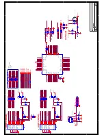
MST6M181VS
U10
MST6M181VS
U10
RESET
3
HOTPLUGA
4
RXCN
5
RXCP
6
RX0N
7
RX0P
8
AVDD_DVI_3.3V
9
RX1N
10
RX1P
11
DDCDA_DA
12
RX2N
13
RX2P
14
DDCDA_CK
15
ARC
16
NC
17
NC
18
NC
19
NC
20
NC
21
NC
22
NC
23
VDDC
24
HSYNC0
25
BIN0P
26
SOGIN0
27
GIN0P
28
GIN0M
29
RIN0P
30
VSYNC0
31
AVDD1P2
32
AVDD2P5_ADC
33
BIN1P
34
SOGIN1
35
GIN1P
36
GIN1M
37
RIN1P
38
AVDD3P3_ADC
39
CVBS4
40
CVBS3
41
CVBS2
42
CVBS1
43
CVBS0
44
VCOM
45
CVBS_OUT1
46
LINEIN_L0
47
LINEIN_R0
48
LINEIN_L1
49
LINEIN_R1
50
VRM
51
VRP
52
VAG
53
AVDD_AU25
54
LINEIN_L3
55
LINEIN_R3
56
LINEIN_L4
57
LINEIN_R4
58
LINEIN_L5
59
LINEIN_R5
60
AVDD_AU33
61
LINEOUT_L3
62
LINEOUT_R3
63
LINEOUT_L0
64
LINEOUT_R0
65
NC
66
NC
67
NC
68
XTAL_IN
69
XTAL_OUT
70
AVDD_DMPLL
71
AVDD25_REF
72
AVSS_PGA
73
VIFM
74
VIFP
75
AVDD25_PGA
76
SIFP
77
SIFM
78
TAGC
79
GPIO22/I2S_OUT_WS/RX2
80
GPIO23/I2S_OUT_SD/TX2
81
GPIO24/TUNER_SCL
82
GPIO25/TUNER_SDA
83
GPIO26/SPDIF_IN/RX1/PWM3
84
GPIO27/SPDIF_OUT
85
VDDC
86
VDDP_1
87
GPIO28
88
GPIO30/I2S_OUT_MCK
89
GPIO32/I2S_OUT_BCK
90
GPIO36
91
GPIO37
92
GPIO38
93
GPIO45
94
GPIO47
95
GPIO49
96
NC
97
B_ODD0/RXE4+
98
B_ODD1/RXE4-
99
B_ODD2/RXE3+
100
B_ODD3/RXE3-
101
B_ODD4/RXEC+
102
B_ODD5/RXEC-
103
B_ODD6/RXE2+
104
B_ODD7/RXE2-
105
G_ODD0/RXE1+
106
G_ODD1/RXE1-
107
AVDD2P5_MOD
108
G_ODD2/RXE0+
109
G_ODD3/RXE0-
110
G_ODD4/RXO4+
111
G_ODD5/RXO4-
112
G_ODD6/RXO3+
113
G_ODD7/RXO3-
114
R_ODD0/RXOC+
115
R_ODD1/RXOC-
116
R_ODD2/RXO2+
117
R_ODD3/RXO2-
118
R_ODD4/RXO1+
119
R_ODD5/RXO1-
120
R_ODD6/RXO0+
121
R_ODD7/RXO0-
122
VDDC
123
AVDD2P5_MOD
124
AVDD_LPLL
125
GPIO74/I2S_IN_WS/PWM4/RX3/LCK
126
GPIO75/I2S_IN_SD/PWM5/TX3/LDE
127
GPIO76/I2S_IN_BCK/PWM2/LHSYNC
128
GPIO77/I2S_OUT_MUTE/PWM3/LVSYNC
129
VDDP_2
130
GPIO20/PWM0
131
GPIO21/PWM1
132
VDDC
133
NC
134
NC
135
A_DDR1_A3
136
A_DDR1_A2
137
A_DDR1_A1
138
A_DDR1_A0
139
A_DDR1_A10
140
A_DDR1_BA1
141
AVDDIO_2.5V
142
A_DDR1_BA0
143
A_DDR1_RAS
144
A_DDR1_CAS
145
A_DDR1_WEZ
146
A_DDR1_DQ0
147
AVDDIO_2.5V
148
A_DDR1_DQ1
149
A_DDR1_DQ2
150
A_DDR1_DQ3
151
A_DDR1_DQ4
152
AVDDIO_2.5V
153
A_DDR1_DQ5
154
A_DDR1_DQ6
155
A_DDR1_DQ7
156
NC
157
NC
158
AVDDIO_2.5V
159
LDQS0
160
LDQM0
161
DVDD_DDR_1.2V
162
AVDD_PLL
163
UDQM0
164
UDQS0
165
A_DDR1_DQ8
166
A_DDR1_DQ9
167
AVDDIO_2.5V
168
A_DDR1_DQ10
169
A_DDR1_DQ11
170
A_DDR1_DQ12
171
A_DDR1_DQ13
172
A_MVREF
173
A_DDR1_DQ14
174
AVDDIO_2.5V
175
A_DDR1_DQ15
176
A_DDR1_MCLKZ
177
AVDDIO_2.5V
178
A_DDR1_MCLK
179
NC
180
A_DDR1_CKE
181
A_DDR1_A12
182
A_DDR1_A11
183
A_DDR1_A9
184
AVDDIO_2.5V
185
A_DDR1_A8
186
A_DDR1_A7
187
A_DDR1_A6
188
A_DDR1_A5
189
A_DDR1_A4
190
VDDC
191
DDCR_DA
192
VDDP_3
193
DDCR_CK
194
TESTPIN
195
DM_P0
196
DP_P0
197
AVDD_NODIE
200
DVDD_NODIE
201
GND_EFUSE
202
SPI_CK
203
SPI_DI
204
SPI_DO
205
SPI_CZ
206
GPIO11/SAR0
207
GPIO12/SAR1
208
GPIO13/SAR2
209
GPIO10/PMGPIO
210
DDCA_CK
211
DDCA_DA
212
GPIO6/PM1/TX
213
GPIO7/PM4/POWER_ON
214
GPIO8/PM5/RX
215
GPIO9/PM6/CS1
216
IRIN
1
CEC
2
E-pad
217
DP_P1
199
DM_P1
198
C213
2.2uF
C213
2.2uF
C57
47n
C57
47n
R10
NC/39K
R10
NC/39K
R202
1K_1%
R202
1K_1%
R26
1M
R26
1M
C149
0.1u
C149
0.1u
R59
200K
R59
200K
R737
68R
R737
68R
R155
10K
R155
10K
C397
2.2uF
C397
2.2uF
R328
1.8K
R328
1.8K
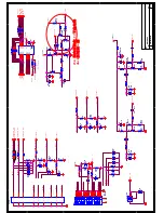
U42
EN25Q32_100HIP
U42
EN25Q32_100HIP
CE#
1
SO
2
WP#
3
VSS
4
SI
5
SCK
6
HOLD#
7
VDD
8
L129
FB
L129
FB
R150
68R
R150
68R
C98
0.1u
C98
0.1u
C129
0.1u
C129
0.1u
C96
0.1u
C96
0.1u
R184
1M
R184
1M
C131
0.1uF
C131
0.1uF
R350
4.7K
R350
4.7K
FB6
FB
FB6
FB
C69
2.2u
C69
2.2u
CN6
CON/4P/P2.54
CON20W-J20-12
CN6
CON/4P/P2.54
CON20W-J20-12
1
2
3
4
5
6
7
8
9
10
11
12
C118
2.2u
C118
2.2u
C134
0.1uF
C134
0.1uF
R32
NC/0
R32
NC/0
C396
2.2uF
C396
2.2uF
C95
0.1u
C95
0.1u
C77
220p
C77
220p
R11
NC/11K
R11
NC/11K
R144
4.7K
R144
4.7K
R156
1K
R156
1K
C127
0.1u
C127
0.1u
R707
4.7K
R707
4.7K
Q21
3904
Q21
3904
1
2
3
C72
2.2u
C72
2.2u
C144
20p
C144
20p
C398
2.2u
C398
2.2u
R149
4.7K
R149
4.7K
VD101
NC
VD101
NC
1
2
Summary of Contents for 8M26S
Page 2: ...Content 2 11 17 18 19 20 21 28 29 45 46 49 50 57 ...
Page 3: ...LED 8M26S ...
Page 5: ...40 55 80 For 22 LED For 24 LED For 32 LED ...
Page 6: ... 24 inches is 3W 24 inches is 4 ohm ...
Page 7: ...40 40 3 2 1 4 2 50 0 5 80 40 3 12000 26inches is 8 ohm ...
Page 8: ...40 YES 8 6 46 46 NO NO Standard Spanish Standard 20 ...
Page 9: ...4 2 4 0 40 70 0 40 70 0 40 40 85 Y0 50 30000 ...
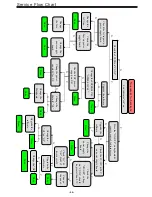
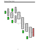
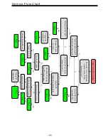
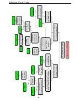
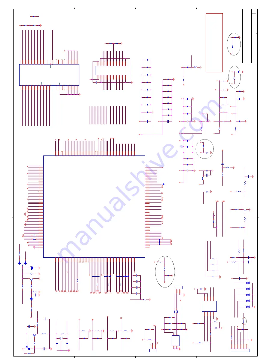
Page 14: ...IC Block Diagram 14 U29 4MX16BIT BANKS DDR M13S2561616A 5TG2K ...
Page 18: ... 18 ...
Page 19: ... 19 Main PCB Top Bottom Layer ...
Page 20: ...Main PCB Top Bottom Layer 20 ...