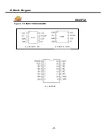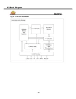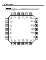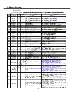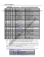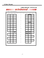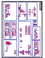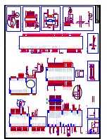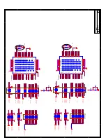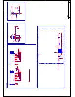
IC Block Diagram
-2
4
-
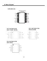
EN25F32
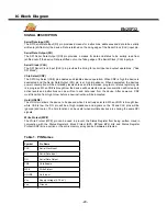
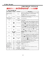
SIGNAL DESCRIPTION
Serial Data Input (DI)
The SPI Serial Data Input (DI) pin provides a means for instructions, addresses and data to be serially
written to (shifted into) the device. Data is latched on the rising edge of the Serial Clock (CLK) input pin.
Serial Data Output (DO)
The SPI Serial Data Output (DO) pin provides a means for data and status to be serially read from
(shifted out of) the device. Data is shifted out on the falling edge of the Serial Clock (CLK) input pin.
Serial Clock (CLK)
The SPI Serial Clock Input (CLK) pin provides the timing for serial input and output operations. ("See
SPI Mode")
Chip Select (CS#)
The SPI Chip Select (CS#) pin enables and disables device operation. When CS# is high the device is
deselected and the Serial Data Output (DO) pin is at high impedance. When deselected, the devices
power consumption will be at standby levels unless an internal erase, program or status register cycle
is in progress. When CS# is brought low the device will be selected, power consumption will increase to
active levels and instructions can be written to and data read from the device. After power-up, CS#
must transition from high to low before a new instruction will be accepted.
Hold (HOLD#)
The HOLD pin allows the device to be paused while it is actively selected. When HOLD is brought low,
while CS# is low, the DO pin will be at high impedance and signals on the DI and CLK pins will be
ignored (don’t care). The hold function can be useful when multiple devices are sharing the same SPI
signals.
Write Protect (WP#)
The Write Protect (WP#) pin can be used to prevent the Status Register from being written. Used in
conjunction with the Status Register’s Block Protect (BP0, BP1and BP2) bits and Status Register
Protect (SRP) bits, a portion or the entire memory array can be hardware protected.
Table 1. PIN Names
Symbol
Pin Name
CLK
Serial Clock Input
DI
Serial Data Input
DO
Serial Data Output
CS#
Chip Enable
WP#
Write Protect
HOLD#
Hold Input
Vcc
Supply Voltage (2.7-3.6V)
Vss
Ground
Summary of Contents for 8M29B
Page 3: ... 3 LCD 8M29B chassis ...
Page 5: ...For 42LED For 42LED 5 8 8 10 15 9800 12500 12500 266 276 9800 280 290 6500 313 329 ...
Page 6: ...40 40 3 2 1 4 2 50 0 5 80 40 12000 6 24 6 ...
Page 8: ... 8 4 ...
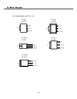
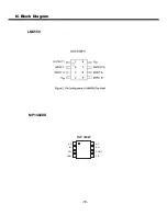
Page 19: ...IC Block Diagram 19 LM4558 MP1482DS BS IN SW GND SS EN COMP FB 1 2 3 4 8 7 6 5 TOP VIEW ...
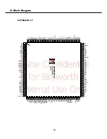
Page 20: ...IC Block Diagram 20 MST6M20S LF ...
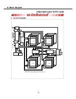
Page 23: ...IC Block Diagram 23 EN25F32 Figure 2 BLOCK DIAGRAM ...
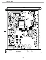
Page 32: ...MAIN PCB TOP 32 ...
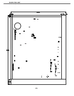
Page 33: ...MAIN PCB BOT 33 ...

