background image

Introduction

http://www.motorola.com/computer/literature

1-15

1

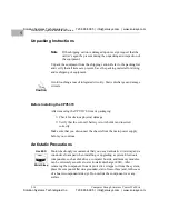
If an ESD station is not available, you can avoid damage resulting from 
ESD by wearing an antistatic wrist strap (available at electronics stores) 
that is attached to an active electrical ground. Note that a system chassis 
may not be grounded if it is unplugged.

Warning

Dangerous voltages, capable of causing death, are present in this 
equipment. Use extreme caution when handling, testing, and adjusting.

Caution

Avoid touching areas of integrated circuitry. Static discharge can damage 
these circuits.

Mounting Memory Mezzanine Cards

You can mount one or two 256MB Memory Mezzanine Modules on the 
CPV5370 Single Board Computer. Refer to 

Antistatic Precautions


on page 

1-14

 before beginning installation. Refer to 

Figure 1-3

.

1. Attach three standoffs to the CPV5370 board and secure with three 

nuts on the secondary side of the board.

2. Place one Memory Mezzanine Module on top of the three standoffs 

and press onto the J16 connector on the CPV5370.

3. Secure with three screws.

If mounting a second Memory Mezzanine Module use a second set 
of three standoffs instead of three screws.

4. Place the second Memory Mezzanine Module on top of the three 

standoffs and press onto the connector on the first Memory 
Mezzanine Module.

5. Secure with three screws.

Solution Systems Technologies Inc.

720-565-5995  |  info@solusys.com  |  www.solusys.com

Solution Systems Technologies Inc.

720-565-5995  |  info@solusys.com  |  www.solusys.com

Summary of Contents for CompactPCI CPV5370-700-01

Page 1: ...cusing on the embedded marketplace We provide custom turnkey solutions to get your project started quickly We pride ourselves in our agility and ability to engineer complex solutions quickly Contact u...

Page 2: ...M04 Transition Module Installation and Reference Guide CPV5370A IH1 May 25 2001 Edition Solution Systems Technologies Inc 720 565 5995 info solusys com www solusys com Solution Systems Technologies In...

Page 3: ...ks of Intel Corporation Windows NT is a registered trademark of Microsoft in the US and other countries CompactPCI is a registered trademark of PCI Industrial Computer Manufacturers Group Phoenix is a...

Page 4: ...tion about Motorola products machines and programs programming or services that are not available in your country Such references or information must not be construed to mean that Motorola intends to...

Page 5: ...ctory Authorized Service Personnel or other qualified service personnel may remove equipment covers for internal subassembly or component replacement or any internal adjustment Service personnel shoul...

Page 6: ...ment of Radio Interference Characteristics of Information Technology Equipment this product tested to Equipment Class A EN50082 1 1997 Electromagnetic Compatibility Generic Immunity Standard Part 1 Re...

Page 7: ...cement incorrect de la batterie Remplacer uniquement avec une batterie du m me type ou d un type quivalent recommand par le constructeur Mettre au rebut les batteries usag es conform ment aux instruct...

Page 8: ...rds 1 15 Mounting PCI Mezzanine Cards 1 16 Mounting the Slim Line EIDE Hard Drive 1 17 Hardware Configuration 1 17 Connecting to Board Connectors 1 18 Installing the CPV5370 Single Board Computer and...

Page 9: ...R 4 Connector Pin Assignments Ethernet Connectors 4 1 Serial Port Connectors 4 3 Video Connector for the CPV5370 J17 and CPTM04 J20 Modules 4 6 Keyboard Mouse P S2 Connector for the CPV5370 and CPTM04...

Page 10: ...J3 J4 and J5 4 19 CPTM04 Transition Module Rear I O Connectors J3 J4 and J5 4 26 APPENDIX A Specifications APPENDIX B Thermal Analysis Measuring Local Air Temperature B 7 APPENDIX C Related Documenta...

Page 11: ...x Solution Systems Technologies Inc 720 565 5995 info solusys com www solusys com Solution Systems Technologies Inc 720 565 5995 info solusys com www solusys com...

Page 12: ...ard Computer and CPTM04 Transition Module in Your Computer Chassis 1 20 Figure B 1 Location of Thermally Significant Components on the CPV5370 Single Board Computer Primary Side B 3 Figure B 2 Locatio...

Page 13: ...xii Solution Systems Technologies Inc 720 565 5995 info solusys com www solusys com Solution Systems Technologies Inc 720 565 5995 info solusys com www solusys com...

Page 14: ...Table 3 11 Bit descriptions for the INTUM register 3 13 Table 3 12 Bit values for determining driven IRQ lines 3 14 Table 3 13 Bit descriptions for the SCIEN register 3 15 Table 3 14 Bit descriptions...

Page 15: ...nsition Module 4 13 Table 4 13 Indicator LED Miscellaneous Connector Pin Assignments on the CPTM04 Transition Module J2 4 15 Table 4 14 IPMI System Management Bus Connector Pin Assignments on the CPTM...

Page 16: ...A 1 Table A 2 Physical Characteristics of the CPV5370 Single Board Computer A 1 Table A 3 Lithium Battery Specifications A 2 Table A 4 Environmental Specifications 1 A 2 Table B 1 Thermally Significa...

Page 17: ...xvi Solution Systems Technologies Inc 720 565 5995 info solusys com www solusys com Solution Systems Technologies Inc 720 565 5995 info solusys com www solusys com...

Page 18: ...0 700 01 CompactPCI SBC with 700MHz processor 256MB SDRAM one PMC site CompactFlash connector CPV5370 700 02 CompactPCI SBC with 700MHz processor 256MB SDRAM one PMC site hard drive CPV5370 700 03 Com...

Page 19: ...o Additional Features on page 1 2 and Input Output Interfaces on page 1 3 for more information about CPTM04 features CPMEZZ Memory Module Model Number Description CPMEZZ 256B 256MB Memory Mezzanine bo...

Page 20: ...al description including information about the PCI Bus the watchdog timer memory address mapping the I O address map and the FPGA registers Chapter 4 Connector Pin Assignments pin assignments for the...

Page 21: ...ntation We want to know what you think about our manuals and how we can make them better Mail comments to Motorola Computer Group Reader Comments DW164 2900 S Diablo Way Tempe Arizona 85282 You can al...

Page 22: ...m III processor and 440GX chip set It can serve either as a standard CompactPCI peripheral CPU or as a system controller The Pentium III processor gives you two USB ports PCI EIDE on board Frame AGP g...

Page 23: ...ng insertion or removal of the CPV5370 and other peripheral CPU slot boards while the chassis is powered up An array of on board I O available from the front panel of the CPV5370 and or the rear panel...

Page 24: ...PTM04 Transition Module Front Panel On board Rear Panel On board Ethernet 1 RJ 45 RJ 45 Ethernet 2 RJ 45 RJ 45 COM1 Serial Port 1 9 pin D sub 10 pin shrouded COM2 Serial Port 2 9 pin D sub PMC Panel P...

Page 25: ...or 100MHz Processor North Intel 440GX Bridge PCI Bridge and Memory Controller Soldered on memory to 512MBx8 Memory mezzanine to 512MBx8 33MHz 64 bit PCI Local Bus Video PMC 1 I O Front Panel PMC FPGA...

Page 26: ...hdog Strobe Status port in ISA I O memory map Assert NMI followed by a system Reset or Soft Reset You can program the watchdog timer via registers in the ISA I O memory map The watchdog timer is prote...

Page 27: ...hronous serial port 9 pin connector one PMC panel keyed for 5 0V PCI video port 15 pin high density D sub connector keyboard mouse circular mini DIN connector board reset push button switch LED indica...

Page 28: ...V5370 Single Board Computer Front Panel 2931 0401 Video PMC site ETHERNET COM 1 ETHERNET Connector Keyboard Mouse Connector Reset LED for Power green Alarm red LED for Hard Disk Drive green Solution S...

Page 29: ...d Computer Connector Description J1 CompactPCI Bus Connector J2 CompactPCI Bus Connector J3 Rear I O CompactPCI Connector J4 Rear I O CompactPCI Connector J5 Rear I O CompactPCI Connector J7 Keyboard...

Page 30: ...Board Components 2926 0301 Slim Line Drive J1 J2 J5 Dual Memory Mezzanine Modules J13 J21 J6 J16 J7 J17 J22 J3 J4 J18 J11 J12 J14 J19 J9 J10 J8 J15 J20 J23 Solution Systems Technologies Inc 720 565 5...

Page 31: ...Connector Description J1 IPMI System Management Bus Connector J3 Rear I O CompactPCI Connector J4 Rear I O CompactPCI Connector J5 Rear I O CompactPCI Connector J10 PIM 64 pin PMC I O connector power...

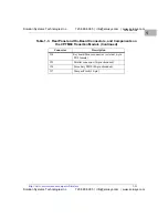
Page 32: ...rouded J26 Secondary EIDE 40 pin shrouded J27 CompactFlash 50 pin Table 1 3 Rear Panel and On Board Connectors and Components on the CPTM04 Transition Module Continued Connector Description Solution S...

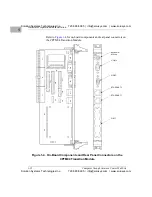
Page 33: ...Module Figure 1 4 On Board Components and Rear Panel Connectors on the CPTM04 Transition Module J19 J18 J14 J10 J21 J26 J25 J5 J4 J3 J20 J22 J24 J16 J23 J15 J17 J1 J27 PIM 1 ETHERNET 2 ETHERNET 1 COM...

Page 34: ...cking the hardware Unpacking Instructions on page 1 14 Mounting memory mezzanine cards Mounting Memory Mezzanine Cards on page 1 15 Mounting PCI Mezzanine Cards PMC Mounting PCI Mezzanine Cards on pag...

Page 35: ...the coin cell battery is in its holder and inserted correctly Make sure that you disconnect the chassis from the main power supply before you continue Antistatic Precautions Use ESD Wrist Strap Motor...

Page 36: ...zanine Modules on the CPV5370 Single Board Computer Refer to Antistatic Precautions on page 1 14 before beginning installation Refer to Figure 1 3 1 Attach three standoffs to the CPV5370 board and sec...

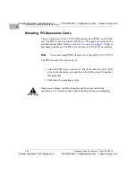
Page 37: ...nterface Note You cannot install PMCs that are only compatible with 3 3V PCI The PMC module I O connects to J3 1 Attach an ESD strap to your wrist Attach the other end of the ESD strap to the chassis...

Page 38: ...e cable to the drive 4 Secure the drive to the CPV5370 using three screws Hardware Configuration To produce the necessary hardware configuration and to make sure the CPV5370 operates properly you may...

Page 39: ...the SBC or TM To reduce the risk of personal injury disconnect the power cord from the power source Only qualified experienced electronics personnel should access the interior of a chassis Caution The...

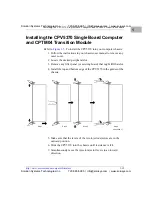
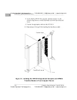
Page 40: ...al slot 3 Remove any filler panel or existing board that might fill that slot 4 Install the top and bottom edge of the CPV5370 in the guides of the chassis 5 Make sure that the levers of the two injec...

Page 41: ...Connect the appropriate cables to the CPV5370 10 Repeat steps 3 through 9 for installing the transition module Figure 1 5 Installing the CPV5370 Single Board Computer and CPTM04 Transition Module in...

Page 42: ...when handling testing and adjusting this equipment and its components Warning Lithium batteries incorporate flammable materials such as lithium and organic solvents If lithium batteries are short circ...

Page 43: ...l ground Note that the system chassis may not be grounded if it is unplugged Secure the ESD strap to your wrist and to ground throughout the procedure 1 To remove the battery from the module carefully...

Page 44: ...pplying power to the system you need to verify that you completed all necessary hardware preparation you made all connections correctly the voltage setting for the chassis power supply matches the vol...

Page 45: ...d Computer SBC front panel This switch is not programmable There are two LED indicators on the CPV5370 SBC front panel left Power green Alarm red right Hard Disk Drive green indicates hard drive activ...

Page 46: ...erence Guide Motorola part number CPV5350A PGx Refer to Jump to User Code in Alternate Flash Bank at the end of this chapter for more information about the CPV5370 BIOS PhoenixBIOS Description The CPV...

Page 47: ...isplay You do however need a keyboard and display to change setup options unless you use the remote setup feature Remote Setup You can change setup options remotely through the BIOS Setup Advanced Men...

Page 48: ...physical connector into a 64 bit High Availability CompactPCI backplane and make connection to off card CompactPCI peripherals through the PCI PCI bridge Peripheral Hot Swap Function The CPV5370 compl...

Page 49: ...F7FFFF 17 5MB Available for PCI 0xFEE00000 0xFEE00FFF 4KB Local APIC Configuration Space 0xFEC10000 0xFEDFFFF 1 94MB Available for PCI 0xFEC00000 0xFEC0FFFF 64KB I O APIC Configuration Space 0x0010000...

Page 50: ...te Keyboard Controller 0070 7 1 bit PIIX4E NMI Enable 0070 6 0 7 bits PIIX4E RTC 0071 1 byte PIIX4E RTC 0072 0073 2 bytes PIIX4E RTC extended registers 0080 008F 16 bytes PIIX4E DMA Page Register 0092...

Page 51: ...y Disk Change Channel 1 03F7 6 0 7 bits Primary IDE Channel Status Port 03F7 write 1 byte Floppy Channel 1 Command 03F8 03FF 8 bytes COM 1 04D0 04D1 2 bytes Interrupt Controller Edge Level Register 0C...

Page 52: ...at offset 07h 0x5Fh Refer to Table 3 4 To access an FPGA register write to the index register first and then read write from the data register The BIOS sets the default FPGA Base address to 58h Table...

Page 53: ...3 5 Map of the FPGA register set DEVICE 00h SYSTEM DEVICE 10h LAN A Ctrl DEVICE 11h LAN B Ctrl DEVICE 14h FLASH Ctrl 00 Status 01 LAN A 01 LAN B 01 FLASH 03 Watchdog 04 INT Sel 05 SCI Mask 06 NMI Mask...

Page 54: ...latched status of the input ENUM Bit 4 ENUM comes from the CPCI bus and signals the insertion of a new device The input is latched when active low and cleared via the LEN register A read of this bit...

Page 55: ...bit descriptions Table 3 7 Bit descriptions for the Watchdog Timer register 7 most significant bit 6 5 4 3 2 1 0 least significant bit CLR_STATUS ALARM_EN SOFT RST WD1 WD0 SEL2 SEL1 SEL0 Solution Sys...

Page 56: ...ast value written Refer to Table 3 9 Table 3 8 Bit values for selecting watchdog timeout time Period SEL2 SEL1 SEL0 46 seconds 0 0 0 93 seconds 0 0 1 3 73seconds 0 1 0 14 91seconds 0 1 1 29 82 seconds...

Page 57: ...he alarm signal not to become active on a watchdog timeout event Read this bit to return the last written value CLR_STATUS Bit 7 Use this bit to reset the watchdog timer output latch Write a logic 1 t...

Page 58: ...efer to Table 3 11 This IRQ can then be generated by a watchdog Timeout or ENUM Table 3 11 Bit descriptions for the INTUM register 7 most significant bit 6 5 4 3 2 1 0 least significant bit RES RES RE...

Page 59: ...RQ Selected 0 0 0 0 No IRQ Selected 0 0 0 1 No IRQ Selected 0 0 1 0 No IRQ Selected 0 0 1 1 No IRQ Selected 0 1 0 0 Select IRQ5 0 1 0 1 No IRQ Selected 0 1 1 0 Select IRQ7 0 1 1 1 No IRQ Selected 1 0...

Page 60: ...et to a logic 1 to allow the generation of an SCI when the ALARM_A or ALARM_B go active Write a logic 0 to these bits to disable an SCI for this event ENUM Bit 4 Set to a logic 1 to allow generation o...

Page 61: ...to allow the generation of an NMI when the ALARM_A or ALARM_B go active Write a logic 0 to this bit to disable an NMI for this event ENUM Bit 4 Set to a logic 1 to allow the generation of an NMI when...

Page 62: ...d ALARM_B Bit 2 Set to a logic 1 to allow the generation of an IRQ when the ALARM_A or ALARM_B go active Write a logic 0 to this bit to disable an IRQ for this event ENUM Bit 4 Set to a logic 1 to all...

Page 63: ...to allow the generation of an Alarm when the ALARM_A or ALARM_B go active Write a logic 0 to this bit to disable an Alarm for this event ENUM Bit 4 Set to a logic 1 to allow the generation of an Alarm...

Page 64: ...ERT input latch Writing a logic 0 has no effect TEMP Bit 1 CPU Temperature Signal This bit is set automatically when a TEMP event is signaled by an off card thermostat device Write a logic 1 to clear...

Page 65: ...c 1 to clear any latched ALARM_A events Writing a logic 0 has no effect ENUM Bit 4 Bus Enumeration Signal This bit is set automatically when an ENUM event occurs Write a logic 1 to clear any ENUM latc...

Page 66: ...he BIOS on the next reset These bits clear at power on and are not affected by reset Software may set these bits by writing 1s to them PBSOFT Bit 7 Use this bit to program the function of the reset pu...

Page 67: ...route LAN A signals to the rear connector The BIOS sets this bit according to CMOS setup ENABLE Bit 7 The BIOS uses this bit to enable LAN A Write a logic 1 to this bit to disable LAN A Write a logic...

Page 68: ...BIOS sets this bit according to CMOS setup FRONT Bit 6 The BIOS uses this bit to route the LAN B signals to either the front or the rear connetors Write a logic 1 to this bit to route LAN B signals t...

Page 69: ...Bit descriptions for the Flash BIOS Control register 7 most significant bit 6 5 4 3 2 1 0 RES RES RES RES RES BC2 BC1 BC0 Table 3 22 Bit selections for the Flash BIOS Device Bank Control 512K BANK Fla...

Page 70: ...7 the BIOS looks for the five character signature _MOT_ in the last five bytes of the selected 512K bank If found the BIOS disables interrupts timers and the watchdog Then it reads the top 64K of the...

Page 71: ...oup Literature Center Web Site Functional Description 3 Solution Systems Technologies Inc 720 565 5995 info solusys com www solusys com Solution Systems Technologies Inc 720 565 5995 info solusys com...

Page 72: ...f your module Ethernet Connectors Refer to Table 4 1 for Ethernet connector pin assignments for the CPV5370 Single Board Computer Ethernet A J10 Ethernet B J9 CPTM04 Transition Module Ethernet 2 J18 E...

Page 73: ...1 Ethernet Connector Pin Assignments for the CPV5370 Single Board Computer and CPTM04 Transition Module Continued Pin Number Signal Mnemonic Signal Description Solution Systems Technologies Inc 720 56...

Page 74: ...1 DCD Data set has detected the data carrier 2 RX Receives serial data input from communications link 3 TX Sends serial output to communications link 4 DTR Indicates that a data set is ready to estab...

Page 75: ...to communication link 4 DTR Indicates that a data set is ready to establish a communication link 5 GND Ground 6 DSR Indicates that a data set is ready to establish a communication link 7 RTS Indicate...

Page 76: ...blish a communications link 3 RX Receives serial data input from communication link 4 RTS UART is ready to exchange data 5 TX Sends serial data to communication link 6 CTS Data set is ready to exchang...

Page 77: ...4 NC no connection 5 DACVSS Video return 6 DACVSS Video return 7 DACVSS Video return 8 DACVSS Video return 9 NC no connection 10 DACVSS Video return 11 NC no connection 12 DDCDAT Display Data Channel...

Page 78: ...ption 1 KBDDAT Data line for keyboard 2 MDAT AUXDAT 1 Data line for mouse 3 GND Keyboard Ground 4 KBDVCC Keyboard Power 5 KBDCLK Clock for keyboard 6 MCLK AUXCLK 2 Clock for mouse 7 CGND Common Ground...

Page 79: ...round 9 GND Ground 10 KBDVCC Keyboard power 11 12 AUXCLK Clock for mouse Table 4 8 USB Connector Pin Assignments for the CPTM04 Transition Module Pin Number Signal Mnemonic Signal Description Pin Numb...

Page 80: ...nitializes the printer 7 D2 Parallel data lines 8 SLIN Selects the printer 9 D3 Parallel data lines 10 GND Ground 11 D4 Parallel data lines 12 GND Ground 13 D5 Parallel data lines 14 GND Ground 15 D6...

Page 81: ...15 Drive data line 19 GND Drive data line 20 21 DMARQ Drive DMA request 22 GND Ground 23 IOW Drive I O write 24 GND Ground 25 IOR Drive I O read 26 GND Ground 27 IORDY Drive is ready for I O cycle s 2...

Page 82: ...elect 32 CS3 Chip select drive 1 also command register block select 8 GND Ground 33 9 GND Ground 34 IOR Drive I O read 10 GND Ground 35 IOW Drive I O write 11 GND Ground 36 VCC 5 Volts 12 GND Ground 3...

Page 83: ...line 48 DD9 Drive data line 24 49 DD10 Drive data line 25 50 GND Ground Table 4 11 CompactFlash Connector Pin Assignments for the CPTM04 Transition Module Continued Pin Number Signal Mnemonic Signal D...

Page 84: ...rack 9 GND Ground 10 MTR0 Motor enable outputs 11 GND Ground 12 DS1 Drive select 1 13 GND Ground 14 DS0 Drive select 0 15 GND Ground 16 MTR1 Motor enable outputs 17 GND Ground 18 DIR Controls the dire...

Page 85: ...k being accessed 33 GND Ground 34 DSKCHG Notifies the disk drive controller that the drive door is open Table 4 12 Floppy Connector Pin Assignments for the CPTM04 Transition Module Continued Pin Numbe...

Page 86: ...Mnemonic Signal Description 1 IDE_LED EIDE primary channel activity LED Connect LED between pins 5 and 6 2 5V 5V DC power 3 PWR_LED Power ON indicator 4 GND Ground 5 PBRESET Push button system reset...

Page 87: ...nal Mnemonic Signal Description 1 SMBCLK System Management Bus Clock 2 GND Ground 3 SMBDAT System Management Bus Data 4 5V 5V dc power 5 N C not connected Table 4 15 CompactFlash Master Slave Connecto...

Page 88: ...O GND AD 12 GND 19 GND AD 13 GND AD 14 AD 15 VCC3 GND 18 GND C BE 1 PAR VCC3 GND SERR GND 17 GND PERR GND RSV RSV VCC3 GND 16 GND LOCK STOP VIO GND DEVSEL GND 15 GND TRDY BD_SEL IRDY FRAME VCC3 GND KE...

Page 89: ...AD 32 GND AD 33 AD 34 AD 35 GND 13 GND AD 36 AD 37 VIO GND AD 38 GND 12 GND AD 39 GND AD 40 AD 41 AD 42 GND 11 GND AD 43 AD 44 VIO GND AD 45 GND 10 GND AD 46 GND AD 47 AD 48 AD 49 GND 9 GND AD 50 AD 5...

Page 90: ...GND 13 GND PMC1 PMC2 PMC3 PMC4 PMC5 GND 12 GND PMC6 PMC7 PMC8 PMC9 PMC10 GND 11 GND PMC11 PMC12 PMC13 PMC14 PMC15 GND 10 GND PMC16 PMC17 PMC18 PMC19 PMC20 GND 9 GND PMC21 PMC22 PMC23 PMC24 PMC25 GND 8...

Page 91: ...izontal synchronization V_VSYNC Vertical synchronization VDDCCLK Display Data Channel clock signal for DDC2 support VDDCDAT Display Data Channel data signal for DDC2 support General GND Ground plane V...

Page 92: ...AD 61 GND 18 GND AD 62 AD 63 PAR64 VCC3 C BE 4 GND 17 GND C BE 5 GND C BE 6 C BE 7 REQ64 GND 16 GND ACK64 AD 0 AD 1 VCC3 AD 2 GND 15 GND AD 3 GND AD 4 AD 5 AD 6 GND Key 11 GND AD 7 GND C BE 0 AD 8 AD...

Page 93: ...1 DSR1 RXD 1 VCC DCD 1 GND 12 GND DTR 2 VCC RI 2 CTS2 RTS 2 GND 11 GND TXD 2 DSR 2 RXD 2 GND DCD 2 GND 10 GND DSKCHG HDSEL RDATA WPROT TR0 GND 9 GND WGATE WDATA STEP DIR MTR1 GND 8 GND DS0 DS1 MTR0 I...

Page 94: ...tem reset output TTL totem pole SM Bus Signals SMBDATA System Management Bus signals SMBCLK SMBALRT EIDE ATA 2 SecondaryChannel TTL levels IOCS16 Indicates a 16 bit register is decoded DMARQ Drive DMA...

Page 95: ...ects the printer STB Data strobe indicates data is valid SLCT Select peripheral indicates it is selected Serial COM Ports 1 and 2 RS232 levels CTS Clear to send DCD Data carrier detected DSR Data set...

Page 96: ...ve track 00 WDATA Write data to drive WGATE Enables head write circuitry of drive WPROT Indicates disk is write protected Universal Serial Bus USB 0 and 1 USB levels UDATAn Signal of differential data...

Page 97: ...12 LANA TD LANA TD GND HS_EJ 14 N C VCC5 VCC5 VCC3 3 VCC3 3 VCC3 3 13 GND PMC1 PMC2 PMC3 PMC4 PMC5 12 N C PMC6 PMC7 PMC8 PMC9 PMC10 11 GND PMC11 PMC12 PMC13 PMC14 PMC15 10 N C PMC16 PMC17 PMC18 PMC19...

Page 98: ...n V_VSYNC Vertical synchronization V_DDCCLK Display Data Channel clock signal for DDC2 support V_DDCDAT Display Data Channel data signal for DDC2 support General GND Ground 5V 5 Volts dc power 3 3V 3...

Page 99: ...PE SLCT 14 N C DTR1 GND RI1 CTS1 RTS1 13 GND TXD1 DSR1 RXD1 5V DCD1 12 N C DTR2 5V RI2 CTS2 RTS2 11 GND TXD2 DSR2 RXD2 GND DCD2 10 N C DSKCHG HDSEL RDATA WPROT TR0 9 GND WGATE WDATA STEP DIR MTR1 8 N...

Page 100: ...2 9A 700MHz with 256 or 512MB SDRAM 3 3V 2 0A 12V 25mA typical 25mA maximum 12V 05A typical 05A maximum Table A 2 Physical Characteristics of the CPV5370 Single Board Computer Parameter Description Fo...

Page 101: ...erating 1 0 G RMS 20 to 2000 Hz random Non operating 6 Gs RMS 20 to 2000 Hz random Altitude Operating 15 000 feet 4 572 m Non operating 40 000 feet 12 192 m Maximum wet bulb Operating 28 C 82 F Non op...

Page 102: ...x gives systems integrators the information necessary to conduct thermal evaluations of the board in a specific system configuration It identifies thermally significant components and lists the corres...

Page 103: ...nter surface of the component air refers to the ambient temperature near the component Table B 1 Thermally Significant Components on the CPV5370 Single Board Computer Reference Designator Generic Desc...

Page 104: ...ermally Significant Components on the CPV5370 Single Board Computer Primary Side 2943 0501 U13 J5 J3 J1 J2 U1 J4 Solution Systems Technologies Inc 720 565 5995 info solusys com www solusys com Solutio...

Page 105: ...ion of Thermally Significant Components on the CPV5370 Single Board Computer Secondary Side J5 J3 J1 J2 J4 2944 0501 U32 Solution Systems Technologies Inc 720 565 5995 info solusys com www solusys com...

Page 106: ...such as a thermal diode For instructions on measuring temperatures using the on board device refer to the CPV5370 Single Board Computer Programmer s Reference Guide Measuring Case Temperature Measure...

Page 107: ...ing a Thermocouple Under a Heatsink HEATSINK BOTTOM VIEW ISOMETRIC VIEW Machined groove for thermocouple wire routing Thermocouple junction bonded to component Heatsink base Thermal pad Through hole f...

Page 108: ...rvative since it includes heating of the air by the component Figure B 4 shows one method of mounting the thermocouple Figure B 4 Measuring Local Air Temperature Thermocouple junction PWB Tape thermoc...

Page 109: ...Group Literature Center Web Site Thermal Analysis B Solution Systems Technologies Inc 720 565 5995 info solusys com www solusys com Solution Systems Technologies Inc 720 565 5995 info solusys com www...

Page 110: ...pful sources of additional information about this product related services and development tools Please note that while these URLs are verified they are subject to change without notice Motorola Compu...

Page 111: ...MG Hot Swap Specification http www picmg org Standard Microsystems Corporation Ultra I O Data Sheet http www smsc com main catalog fdc37c67x html Wired for Management PXE Preboot Execution Environment...

Page 112: ...OS write protect control register 3 24 FPGA descriptions 3 7 FPGA registers 3 6 functional description 3 1 functions 1 5 H headless operation 3 2 humidity A 2 I I O address map 3 5 input output interf...

Page 113: ...15 register descriptions 3 7 registers alarm enable 3 18 Flash BIOS write protect control 3 24 interrupt select 3 13 IRQ enable 3 17 LAN A control 3 22 LAN B control 3 23 latch enable 3 19 NMI enable...

Page 114: ...cusing on the embedded marketplace We provide custom turnkey solutions to get your project started quickly We pride ourselves in our agility and ability to engineer complex solutions quickly Contact u...

Reviews: