SN8P2711A
8-Bit Micro-Controller
SONiX TECHNOLOGY CO., LTD
Page 46
Version 0.1
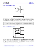
3.6.4 Voltage Bias Reset Circuit
MCU
VDD
VSS
VCC
GND
RST
R1
47K ohm
R3
2K ohm
R2
10K ohm
Q1
E
C
B
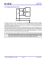
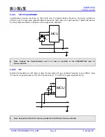
The voltage bias reset circuit is a low cost voltage detector and can
improve brown out reset condition completely
.
The operating voltage is not accurate as zener diode reset circuit. Use R1, R2 bias voltage to be the active level. When
VDD voltage level is above or equal to “0.7V x (R1 + R2) / R1”, the C terminal of the PNP transistor outputs high
voltage and MCU operates normally. When VDD is below “0.7V x (R1 + R2) / R1”, the C terminal of the PNP transistor
outputs low voltage and MCU is in reset mode.
Decide the reset detect voltage by R1, R2 resistances. Select the right R1, R2 value to conform the application. In the
circuit diagram condition, the MCU’s reset pin level varies with VDD voltage variation, and the differential voltage is
0.7V. If the VDD drops and the voltage lower than reset pin detect level, the system would be reset. If want to make the
reset active earlier, set the R2 > R1 and the cap between VDD and C terminal voltage is larger than 0.7V. The external
reset circuit is with a stable current through R1 and R2. For power consumption issue application, e.g. DC power
system, the current must be considered to whole system power consumption.
Note: Under unstable power condition as brown out reset, “Zener diode rest circuit” and “Voltage bias
reset circuit” can protects system no any error occurrence as power dropping. When power drops
below the reset detect voltage, the system reset would be triggered, and then system executes
reset sequence. That makes sure the system work well under unstable power situation.

