C702
1221-7857 rev. 1
FUNCTIONAL OVERVIEW
FU
N
C
T
IO
N
A
L O
V
E
R
V
IE
W
Technical Description
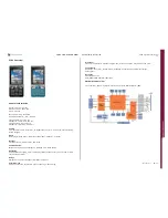
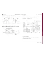
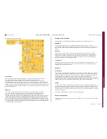
WCDMA Transceiver Block Diagram:
Transmitter
The TX IQ modulator has differential voltage I and Q inputs. It converts input signals to
RF output frequency and is designed to achieve LO and image suppression.
The transmit output stage provides at least +5 dBm at maximum power control at the
differential output. Gain is set through the 3-wire bus. Two 10-bit DAC are used to control the
DC/DC converter and the PA gain. Those DACs are controlled through the 3-wire-bus. One 11-
bit DAC is used to control the variable gain output of the transceiver chip. The transceiver chip
output feeds the constant gain power amplifier, which means that the transceiver chip sets the
phone’s output power.
Receiver
The receiver converts the antenna RF signal down to a Zero Intermediate Frequency
(ZIF). The first stage after the duplexer is a single-ended LNA with a 23 dB gain step.
This LNA is followed by a SAW filter. The LNA and SAW filter are integrated in the
LNA/SAW module. The output from the LNA/SAW module goes to the input of the N300 circuit
(Inside the Mammoth module) and is buffered by an amplifier and then sent to the IQ down-
mixer, which consists of two mixers in parallel driven by quadrature phase LO signals. The In
phase (I) and Quadrature phase (Q) ZIF signals are then low pass filtered to provide protection
from high frequency offset interferer and fed into the channel filter. The front-end zero IF I and
Q outputs are applied to the integrated low-pass channel filter. The filter is self-calibrated with
a cut-off frequency around 2.15 MHz.
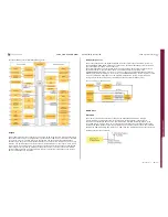
Bluetooth and FM Radio
The STLC2592 circuit N1400 combines Bluetooth and FM tuner functionality into one.
Bluetooth
The Bluetooth implementation is compliant with Bluetooth specification 2.1 + EDR.
The Bluetooth
TM
transceiver has frequency channels with 1 MHz separation from 2402 to 2480
MHz. The same band is used for both transmission and reception. This gives 79 frequency
channels.
Receiver
The first stage of the receiver is an external antenna filter, which suppresses unwanted
frequencies. The receiver is of a “near-zero” IF receiver architecture. The local oscillator is
generated by a frequency synthesizer, which allows the receiver to be set at frequencies in
intervals of 1 MHz. The synthesizer is controlled from the logic part. The received signal is
sampled in the logic for later signal processing.
Transmitter
The synthesizer generates the TX frequency which modulated by the BT baseband block. It is
then amplified. The BT system is a class 1 device with maximum of +4 dBm output power
(minimum setting is about -50 dBm).
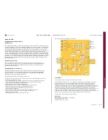
FM Radio
FM Receiver
The receiver uses a digital low-IF architecture. The receive (RX) section integrates a low noise
amplifier (LNA) supporting the worldwide FM broadcast band (76 to 108 MHz). An automatic
gain control (AGC) circuit controls the gain of the LNA to optimize sensitivity and rejection of
strong interferers. An image-reject mixer down converts the RF signal to low-IF.
The quadrature mixer output is amplified, filtered and digitized with high resolution analog-to-
digital converters (ADCs). This advanced architecture allows the use of digital signal processing
(DSP) to perform channel selection, FM demodulation and stereo audio processing.
Tuning
The receiver uses frequency synthesizer technology including a completely integrated VCO. The
frequency synthesizer generates the quadrature local oscillator signal used to downconvert the
RF input to a low intermediate frequency. The VCO frequency is locked to the reference clock
and adjusted with an automatic frequency control (AFC) servo loop during reception. The tuning
frequency is defined as:
Freq (MHz) = Spacing (kHz) × C Bottom of Band (MHz)
External Connectors
External units are connected to the transceiver by means of a 12-pin connector on the bottom
of the phone.
SEMC Troubleshooting Manual
93
(115)
Summary of Contents for C702
Page 116: ...www s manuals com ...

