C905
1222-9526 rev. 1
APPENDIX
A
P
P
E
NDIX
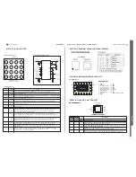
Components - N1210, N1211, N1510, N2200
REFBP
AGND
LDO2
IN2
REFIN
EN2
IN1B
PA_EN
(BUMP IN BOTTOM)
16-Bump, 2mm
×
2mm WLP
HP
LDO1
PAB
EN1
PGND
LX
IN1A
PAA
A1
A2
A3
A4
B1
B4
B3
B2
C1
C2
C3
C4
D1
D4
D3
D2
TOP VIEW
Pin Configuration
Pin Description
PIN
NAME
FUNCTION
A1
REFBP
Reference Noise Bypass. Bypass REFBP to AGND with a 0.22μF ceramic capacitor to reduce noise on the
LDO outputs. REFBP is internally pulled down through a 1k
Ω
resistor during shutdown.
A2
AGND
Low-Noise Analog Ground
A3
REFIN
DAC-Controlled Input. The output of the PA step-down converter is regulated to 2 x V
REFIN
. When V
REFIN
reaches 0.465 x V
IN2
, bypass mode is enabled.
A4
PGND
Power Ground for PA Step-Down Converter
B1
LDO2
200mA LDO Regulator 2 Output. Bypass LDO2 with a 1μF ceramic capacitor as close as possible to LDO2
and AGND. LDO2 is internally pulled down through a 1k
Ω
resistor when this regulator is disabled.
B2
PA_EN
PA Step-Down Converter Enable Input. Connect to IN_ or logic-high for normal operation. Connect to GND
or logic-low for shutdown mode.
B3
EN2
LDO2 Enable Input. Connect to IN2 or logic-high for normal operation. Connect to AGND or logic-low for
shutdown mode.
B4
LX
Inductor Connection. Connect an inductor from LX to the output of the PA step-down converter.
C1
IN2
Supply Voltage Input for LDO1, LDO2, and Internal Reference. Connect IN2 to a battery or supply voltage
from 2.7V to 5.5V. Bypass IN2 with a 2.2μF ceramic capacitor as close as possible to IN2 and AGND.
Connect IN2 to the same source as IN1A and IN1B.
C2
HP
High-Power Mode Set Input. Drive HP high to invoke forced bypass mode. Bypass mode connects the
input of the PA step-down converter directly to its output through the internal bypass MOSFET. Drive HP
low to disable the forced bypass mode.
C3, C4
IN1B,
IN1A
Supply Voltage Input for PA Step-Down Converter. Connect IN1_ to a battery or supply voltage from 2.7V to
5.5V. Bypass the connection of IN1_ with a 2.2μF ceramic capacitor as close as possible to IN1_, and
PGND. IN1A and IN1B are internally connected together. Connect IN1_ to the same source as IN2.
D1
LDO1
200mA LDO Regulator 1 Output. Bypass LDO1 with a 1μF ceramic capacitor as close as possible to LDO1
and AGND. LDO1 is internally pulled down through a 1k
Ω
resistor when this regulator is disabled.
D2
EN1
LDO1 Enable Input. Connect to IN2 or logic-high for normal operation. Connect to AGND or logic-low for
shutdown mode.
D3, D4
PAB, PAA
PA Connection for Bypass Mode. Internally connected to IN1_ using the internal bypass MOSFET during
bypass mode. PA_ is connected to the internal feedback network. Bypass PA_ with a 2.2
μF ceramic
capacitor as close as possible to PA_ and PGND.
IN1A
LX
PAA
1
μ
H
BATT
2.7V TO 5.5V
AGND
PA_EN
REFIN
EN1
EN2
IN2
BATT
2.7V TO 5.5V
PA ON/OFF
ANALOG CONTROL
V
PA
0.4V TO V
BATT
REFBP
IN1B
LDO1 ON/OFF
LDO2 ON/OFF
PAB
LDO2
LDO1
V
LDO2
UP
TO 200mA
PGND
HP
FORCED BYPASS
2.2
μ
F
2.2
μ
F
V
LDO1
UP
TO 200mA
T ypical Operating Circuit
N1210 IC Linear 1203-5870
N1211 LDO Regulator 300mA Low Noise 1204-5903
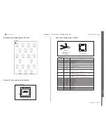
Pin configuration
Pin assignment:
1 - GND
2 - Bluetooth
3 - Vc1 (switch control)
4 - Vc2 (switch control)
5 - Vc3 (switch control)
6 - Power detector output
7 - RXb (balanced)
8 - RXa (balanced)
9 - Vref PA
10 - GND
11 - TX
12 - GND
13 - GND
14 - GND
15 - GND
16 - Vcc PA
17 - ANT
18 - GND
19 - GND (center ground pad)
ANT
14
Top View
15
13
16
Vcc PA
19
RXa
Vc2
10
12
11
17
18
2
1
3
6
4
5
9
8
7
Vref PA
Vc3
RXb
Vc1
D
P
T
B
ANT
14
Top View
15
13
16
Vcc PA
19
RXa
Vc2
10
12
11
17
18
2
1
3
6
4
5
9
8
7
Vref PA
Vc3
RXb
Vc1
D
P
T
B
N1510 Mod Radio WLAN R041D 1200-6173
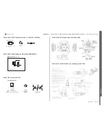
PIN ASSIGNMENTS
DRV PACKAGE
MODE
FB
GND
SW
EN
VIN
1
2
3
6
5
4
r
Pow
e
PAD
TERMINAL FUNCTIONS
TERMINAL
I/O
DESCRIPTION
NAME
NO.
V
IN
5
PWR
VIN power supply pin.
GND
6
PWR
GND supply pin
This is the enable pin of the device. Pulling this pin to low forces the device into shutdown mode. Pulling
EN
4
I
this pin to high enables the device. This pin must be terminated.
This is the switch pin and is connected to the internal MOSFET switches. Connect the external inductor
SW
1
OUT
between this terminal and the output capacitor.
Feedback Pin for the internal regulation loop. Connect the external resistor divider to this pin. In case of
FB
3
I
fixed output voltage option, connect this pin directly to the output capacitor
MODE pin = high forces the device to operate in fixed-frequency PWM mode. Mode pin = low enables
MODE
2
I
the Power Save Mode with automatic transition from PFM mode to fixed-frequency PWM mode.
N2200 IC Vreg SON 6-pin 1204-4655
SEMC Troubleshooting Manual
104
(124)


