C905
1222-9526 rev. 1
FUNCTIONAL OVERVIEW
FU
N
C
T
IO
N
A
L O
V
E
R
V
IE
W
Technical Description
Frequency Generation
The 26 MHz reference signal is used as the reference for the on-chip synthesizers. To
cover the required frequency range, the integrated Voltage Controlled Oscillator (VCO)
operates at twice the frequency for band 1800/1900/2100, and at four times the desired
frequency for band 800/900. The two synthesizers are controlled through the serial bus
from the access side of the digital baseband controller.
EDGE/GPRS/GSM Transmitter Part
Polar modulation transmitter architecture based on the direct phase/frequency
modulation/synthesizer architecture is implemented for GSM, GPRS and EDGE. This
architecture has the capability of generating both the GSM/GPRS constant envelope
GMSK modulation and the linear EDGE 8-PSK modulation in a very cost efficient way.
The motivation for a polar modulation transmitter architecture compared to traditionally
linear architectures is to reduce the output noise (thus eliminating the need for off-chip
filters) reduce the power consumption by utilizing non-linear switching analog signal
processing blocks, and to eliminate the need for an RF isolator.
In brief, the phase/frequency modulator in this polar modulation architecture is a sigma-
delta controlled fractional-N frequency synthesizer with an additional frequency insertion
point after the loop filter at the input of the VCO. The Phase-locked Loop (PLL) has two
information inputs: the divider ratio in the feedback path and a direct path to the VCO.
The phase locked loop generates the radio frequency carrier including the phase
modulation information at the desired channel frequency.
WCDMA Transmitter Part
The WCDMA transmitter architecture is an on frequency linear direct up-conversion IQ-
modulator. The in-phase and quadrature-phase reconstruction filters are fully integrated
and a programmable gain amplifier implements the gain control. An external SAW filter
between the WCDMA circuit and the power amplifier is used to improve noise
performance. After the power amplifier, the signal is sent through an isolator and
through the duplex filter, which directs the transmit signal to the antenna connector
through the antenna switch. The supply voltage and bias of the power amplifier are
adapted depending on the output power to achieve high efficiency at every transmitter
power level. A high efficiency DC/DC converter regulates the supply voltage and the bias
operation point is controlled by a D/A-converter in the WCDMA radio circuit.
Receiver Part
The receiver architecture is a direct down-conversion zero-IF receiver with integrated
low-pass filters. The complete receiver with seven Low Noise Amplifiers (LNAs), one for
each supported band, is integrated on chip. After the down-conversion, the in-phase and
quadrature-phase components are low pass filtered and if the receiver is in
EDGE/GPRS/GSM mode the signals are fed to the integrated high dynamic range sigma-
delta A/D-converters.
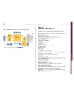
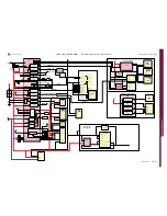
Ericsson RF 3300 Block Diagram:
SEMC Troubleshooting Manual
94
(124)


