background image

HCD-EC59/EC590

10

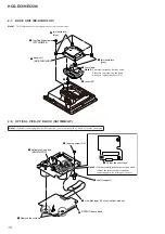
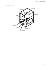
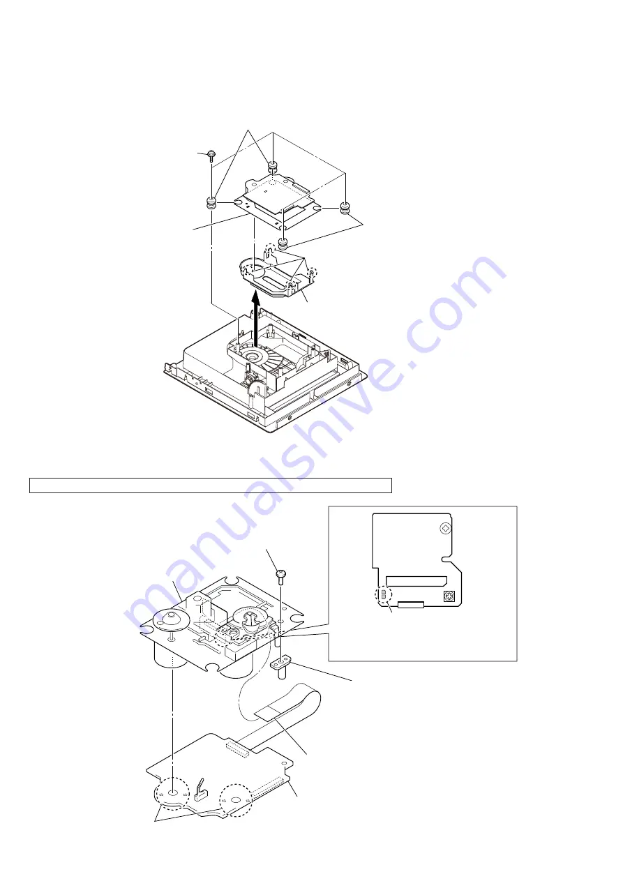
2-7.  BASE  UNIT (BU-D1BD74UR)

Note 1:

 This illustration sees the top panel assy from base unit side.

1

 four floating screws

 (PTPWHM2.6)

4

 two insulators

 (blue)

3

 two insulators

 (gray)

5

 four claws

6

 cover (D1)

7

 base unit

 (BU-D1BD74UR)

2

Note 2:

 Four claws might be fixed by bond.


Please fix four claws by the bond


when you replace the cover (D1).

3

 wire (flat type) (16 core) (optical pick-up)

1

 Remove four solders.

2

 Solder the short-land.

4

 BD74UR board block

7

 optical pick-up block

 (DA11MMVGP)

5

 tapping screw (P2)

6

 shaft (support)

Note 2:

 When assembling the optical pick-up block, 


remove the solder of short-land after 


connecting the wire (flat type) (16 core).

2-8.  OPTICAL  PICK-UP  BLOCK (DA11MMVGP)

Note 1:

 When disconnecting the wire (

fl

 at type) (16 core) of optical pick-up block, solder the short-land.

Summary of Contents for Argentina HCD-EC590

Page 1: ...o mini jack accepts headphones with an impedance of 8 Ω or more SPEAKERS impedance 6 Ω USB section Supported bit rate MP3 MPEG 1 Audio Layer 3 32 kbps 320 kbps VBR WMA 48 kbps 192 kbps AAC 48 kbps 320 kbps Sampling frequencies MP3 MPEG 1 Audio Layer 3 32 44 1 48 kHz WMA 44 1 kHz AAC 44 1 kHz USB port Maximum current 500 mA CD player section System Compact disc and digital audio system Laser Diode ...

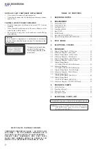
Page 2: ...AL PARTS LIST 36 Accessories are given in the last of the electrical parts list TABLE OF CONTENTS NOTES ON CHIP COMPONENT REPLACEMENT Never reuse a disconnected chip component Notice that the minus side of a tantalum capacitor may be dam aged by heat FLEXIBLE CIRCUIT BOARD REPAIRING Keep the temperature of soldering iron around 270 C during repairing Do not touch the soldering iron on the same con...

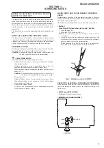
Page 3: ... break down and also use the procedure in the printed matter which is included in the repair parts The flexible board is easily damaged and should be handled with care NOTES ON LASER DIODE EMISSION CHECK The laser beam on this model is concentrated so as to be focused on the disc reflective surface by the objective lens in the optical pickup block Therefore when checking the laser diode emission o...

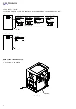
Page 4: ... number plate or the sculpture of back panel MAIN board Rear side view Argentina Mexican and African models Argentina model 4 184 199 0s AR 4 290 683 0s AR Mexican model 4 184 200 0s MX African model Argentina model 4 184 201 0s E4 Back Panel MODEL NUMBER LABEL EC59 MODEL NUMBER PLATE EC590 120V AC area in E model Chilean and Peruvian models Sculpture Back Panel Ver 1 1 ...

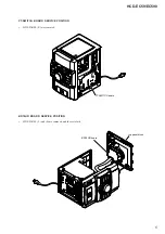
Page 5: ...HCD EC59 EC590 5 PT SWITCH BOARD SERVICE POSITION SIDE PANEL R was removed BD74UR BOARD SERVICE POSITION SIDE PANEL L and R are removed and the set is laid PT SWITCH board top panel block BD74UR board ...

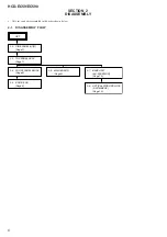
Page 6: ...assembled in the order shown below 2 1 DISASSEMBLY FLOW SET 2 6 MAIN BOARD Page 9 2 3 TOP PANEL ASSY Page 7 2 2 SIDE PANEL L R Page 7 2 4 FRONT PANEL BLOCK Page 8 2 5 KNOB VOL Page 8 2 8 OPTICAL PICK UP BLOCK DA11MMVGP Page 10 2 7 BASE UNIT BU D1BD74UR Page 10 ...

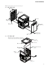
Page 7: ...y in the back and remove the two claws in front of the top panel assy 7 top panel assy 4 flexible flat cable 25 core CN403 Note Follow the disassembly procedure in the numerical order given 2 2 SIDE PANEL L R 2 two screws BVTP3 u 10 5 side panel L 5 side panel R 1 three screws case 3 TP2 4 two claws 3 3 2 two screws BVTP3 u 10 1 three screws case 3 TP2 4 two claws ...

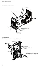
Page 8: ...hole 2 Push the knob VOL by flat head screwdriver front panel block PANEL board 1 flexible flat cable 25 core CN901 2 4 FRONT PANEL BLOCK 8 front panel block 6 claw 1 flexible flat cable 25 core CN607 2 flexible flat cable 9 core CN605 5 three screws BVTT3 u 8 4 lead wire from USB board 3 screw BVTP3 u 10 7 6 claw ...

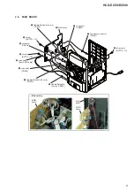
Page 9: ...lexible flat cable 9 core CN605 1 flexible flat cable 25 core CN607 8 two screws BVTP3 u 10 7 fan motor connector CN601 9 lead wire from USB board 6 connector CN633 4 connector CN604 3 connector CN609 8 screw BVTP3 u 10 8 screw BVTP3 u 10 0 MAIN board MAIN board MAIN board back panel ...

Page 10: ...x four claws by the bond when you replace the cover D1 3 wire flat type 16 core optical pick up 1 Remove four solders 2 Solder the short land 4 BD74UR board block 7 optical pick up block DA11MMVGP 5 tapping screw P2 6 shaft support Note 2 When assembling the optical pick up block remove the solder of short land after connecting the wire flat type 16 core 2 8 OPTICAL PICK UP BLOCK DA11MMVGP Note 1 ...

Page 11: ... Press the 1 button to turn the power on 2 Press the FUNCTION button to select CD function 3 Press the 1 button again to turn the power off standby 4 After pressing the DISPLAY button while pressing the x button press the 1 button 5 It turns power on and display CD USB then display PWR ON or PWR OFF CHANGE OVER THE AM TUNING INTERVAL The AM tuning interval can be changed over 9 kHz or 10 kHz Proce...

Page 12: ...CTORY is displayed When the CD button is pressed the following message initial display is displayed ON S character mode setting Tracking servo setting RF gain setting Key Operation CD The display changes in the following order when ever the button is pressed DSGX RF gain setting changes whenever the button is pressed No gain fixation AL Fix to the gain for AL disc RW Fix to the gain for RW disc FU...

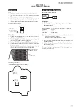
Page 13: ... oscilloscope waveform is as shown in the figure below eye pattern A good eye pattern means that the diamond shape in the center of the waveform can be clearly distinguished VOLT DIV 200 mV TIME DIV 500 ns level 1 1 0 4 Vp p Checking Location CL102 RFOUT CL117 VREF IC101 IC301 BD74UR Board Conductor Side TUNER SECTION 0 dB 1 μV FM AUTO STOP CHECK signal generator set Procedure 1 Turn the power on ...

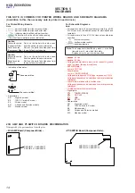
Page 14: ...can model For Printed Wiring Boards Note X parts extracted from the component side Y parts extracted from the conductor side W indicates side identified with part number Pattern from the side which enables seeing The other layers patterns are not indicated Indication of transistor C B These are omitted E Q B These are omitted C E Q Caution Pattern face side Conductor Side Parts face side Component...

Page 15: ...HCD EC59 EC590 15 Circuit Boards Location USB board REG board BD74UR board MAIN board JACK board PANEL board PT SWITCH board 2CH AMP board USB JACK board ...

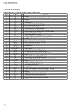
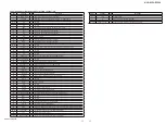
Page 16: ... Power supply terminal 3 3V 20 VSS2 Ground terminal 21 22 P00 P01 I O Not used 23 to 25 DBGP0 to DBGP2 Debug terminal 26 SDAT I Serial data input from the CD MP3 processor 27 BCLK I Bit clock signal input from the CD MP3 processor 28 LRCK I L R sampling clock signal input from the CD MP3 processor 29 30 P20 P21 I O Not used 31 P22 O Audio serial data output to the CD MP3 processor 32 P23 O Request...

Page 17: ... control signal output to the USB controller 34 O USB RST O System reset signal output to the USB controller 35 AVSS Ground terminal 36 I P MONI I Power monitor signal input terminal 37 38 I KEY1 I KEY2 I Front panel key input terminal A D input 39 I TU ANSD I Auto gain control signal input terminal 40 I 5V 9V DET I Power supply voltage detection signal input terminal 41 I KEY WAKE UP VOL I Front ...

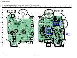
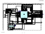
Page 18: ... C203 C205 CL101 CL102 CL103 CL104 CL105 CL106 CL107 CL108 CL109 C418 CL110 CL111 CL112 CL113 CL114 CL115 CL116 CL117 CL118 CL119 S001 LIMIT M401 SPINDLE M402 SLED CL120 CL121 SL301 SL302 SL303 SL304 R101 R102 R103 R104 R105 R106 R107 R108 R109 R301 R302 R303 R304 R111 R305 R112 R113 R114 R116 R118 R120 R122 R123 R124 R126 R129 R131 C101 C102 C103 C104 1 20 21 40 41 60 61 80 C105 C106 C107 C108 C3...

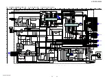
Page 19: ...201 F T T F MD VR LD GND F C B A D E VCC VREF 2SA2119K Q201 16 934MHz X101 S001 LIMIT C203 10 C205 10 0 1 C201 10V 100 C207 1 C206 1000p C208 0 1 C209 1 R201 2 2 R202 330 R101 4700p C101 0 01 C102 0 1 C103 0 1 C104 0 1 C107 0 01 C105 3300p C106 0 01 C108 0 22 C110 0 022 C111 0 1 C112 0 047 C117 10k R102 0 R103 0 R104 0 R105 0 R106 68k R107 1k R108 1k R109 22k R111 0 R112 680 R113 680 R114 68k R116...

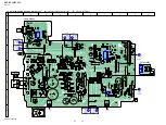
Page 20: ...925 CL926 CL927 CL928 CL932 CL929 CL930 CL931 CL933 CL934 CL935 CL936 R900 R901 R902 R903 R904 R905 R906 R907 R908 R909 R910 R911 R912 R913 R914 R915 R916 R917 R918 R919 CN901 24 25 24 1 2 25 2 1 CN902 CN903 R920 R921 R922 R923 R924 CN910 C900 C901 C902 C903 C904 C905 C906 C907 C908 C909 W961 X901 W962 R951 C915 R952 C916 R953 C917 R954 C918 R955 C919 C920 C921 C950 C951 C952 C953 C954 C955 IC901 ...

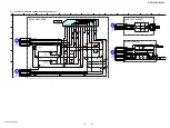
Page 21: ... 22p C902 22p C903 1 2 3 4 5 6 7 8 9 10 11 12 13 14 15 16 17 18 19 20 21 22 23 24 25 25P CN901 VBUS5V VBUS5V VBUS5V VBUSGND VBUSGND VBUSGND USB RST USB RXD USB TXD USB SLEEP CD CE CD CL CD DI CD DO CD RST CD M MUTE DVDD3 3V DGND AGND CD USB Lch AU GND CD USB Rch AVDD3 3V CD VM7V CD M GND CL903 CL934 CL935 LC87F1JJ2AU SQFP H IC901 USB CONTROLLER 1 P73 2 RES 3 XT1 4 XT2 5 VSS1 6 CF1 7 CF2 8 VDD1 9 S...

Page 22: ...8 R791 R792 R793 R794 R795 R796 R797 R798 Q604 R799 Q605 Q606 Q608 D701 C763 C765 C766 Q611 Q612 TP660 Q618 TP661 Q619 TP662 TP663 TP664 TP665 C776 TP666 TP667 TP668 TP669 L801 L802 TP670 TP671 IC701 TP672 TP673 TP674 TP675 TP676 TP677 C788 TP678 C789 TP679 D731 D732 D735 1 3 1 3 4 5 1 2 1 8 1 2 8 9 E B E B 2 1 24 25 3 1 B E 1 5 TB602 LP002 LP003 CN601 CN603 CN604 CN605 CN607 CN609 CN801 R638 R641...

Page 23: ...TP675 TP677 TP674 1 2 3 3P CN609 IN GND OUT R879 100 C852 0 01 8 7 6 5 4 3 2 1 NJM2368V TE2 IC701 IN FB GND OUT V CS CT REF 1N4002 A2 D611 1N4002 A2 D612 1N5402 C532 2 D607 1N5402 C532 2 D608 1N5402 C532 2 D609 1N5402 C532 2 D610 27k R689 0 1 C715 3 3 R767 68k R657 470 R673 470 R688 1000p C694 3300p C662 C763 470p R770 100k C766 4700p R782 10k 25V 1000 C628 E ET601 E ET602 C621 0 1 C623 0 1 TP615 ...

Page 24: ...C101 C102 C109 C110 C162 C163 IC102 TP559 TP560 TP561 TP562 FB561 FB562 R561R562 C565 1 4 1 4 CN560 CN561 C561 JW560 R477 R478 C491 C495 C496 TP491 TP492 TP493 TP494 TP495 TP496 TP497 TP498 1 2 8 9 CN496 JW491 JW492 J491 J492 J1 MAIN BOARD CN633 K1 MAIN BOARD CN603 2CH AMP BOARD 1 882 028 11 11 J2 MAIN BOARD CN633 K2 MAIN BOARD CN603 2CH AMP BOARD 1 882 028 12 12 C USB BOARD CN903 1 882 031 11 12 ...

Page 25: ... C110 47 R107 47k 220 R163 1k R120 R116 1 5k R115 1 5k 0 1 C165 0 1 C164 R105 2 2k R106 2 2k 5P W102 1 PA GND 2 LOW OUT R 3 VH 4 VH 5 LOW OUT L R104 2 2k R103 2 2k 50V C163 100 50V 100 C162 1 9 8 7 6 5 4 3 2 15 14 13 12 11 10 IC102 STK433 040 PRE VCC VCC PRE SUB GND ST BY C141 0 1 C142 0 1 0 1 C112 IC102 2CH POWER AMP 2CH AMP BOARD OVERLOAD DETECT OVERLOAD DETECT E 3 D 7 8 9 10 11 12 13 A C 4 2 6 ...

Page 26: ... R378 R379 C340 C341 C342 R381 R382 R383 R384 R390 R391 R392 C356 R396 D301 D302 D303 D304 JR306 JR309 IC301 Q452 B E 1 2 24 25 1 2 11 10 B E 1 37 24 2 25 1 1 2 JW370 JW371 JW372 JW374 JW375 JW376 JW377 JW378 JW382 JW386 SW471 SW472 SW473 R454 SW474 R455 SW475 R456 SW476 LCD301 SW481 SW482 SW483 SW484 SW485 SW486 SW487 CN451 SW491 C451 C452 C454 Q302 D400 W305 D452 D453 S491 CN301 CN305 C302 C303 ...

Page 27: ...TE O USB RXD AVCC O USB SLEEP O USB RST AVSS I P MONI I KEY1 I KEY2 I TU ANSD I 5V 9V DET I KEY WAKE UP VOL I HOLD NC GND NC I MODEL I SUFFIX I TU DO O I2C FUNC DATA O I2C FUNC CLK MD2 MD1 MD0 I RST O TU CE O TU DI O TU CLK VLCD COM0 COM1 CMO2 CMO3 SEG0 SEG1 VCC VSS SEG2 SEG3 SEG4 SEG5 SEG6 SEG7 SEG8 SEG9 SEG10 SEG11 SEG12 SEG13 SEG14 SEG15 SEG16 SEG17 SEG18 SEG19 SEG20 SEG21 SEG22 SEG23 SEG24 VCC...

Page 28: ...s unleaded solder See page 15 for Circuit Boards Location 5 11 PRINTED WIRING BOARD PT SWITCH Board SUFFIX 11 5 12 PRINTED WIRING BOARD PT SWITCH Board SUFFIX 12 C051 D051 D052 D053 1 3 1 8 W052 CN051 JW003 JW004 JW006 JW007 JW008 PT051 JW009 PT054 JW011 JW012 JW013 JW014 JW015 JW016 JW017 JW018 JW019 JW020 S051 RY051 RY052 MAIN POWER TRANSFORMER SUB POWER TRANSFORMER 1 4 9 5 1 6 14 10 AC IN E1 MA...

Page 29: ... MC2838 T112 1 D052 PT054 3 11 12 13 14 5 10 2 4 6 JW004 C051 0 1 MC2836 T112 1 D051 RY052 JW009 1 2 3 4 5 6 7 8 8P W052 RELAY ON OFF V STBY AC DETECT VH AC VL AC GND VL AC VH AC JW011 1 SUB POWER TRANSFORMER TRANSFORMER MAIN POWER BUILT IN TRANSFORMER NOT REPLACEABLE 220V 230 240V 120V PT SWITCH BOARD 1 2 VOLTAGE SELECTOR E2 E4 E51 AR EXCEPT MX MX AC IN E 3 D F 8 7 A C 4 2 6 B 5 1 PT054 Page 23 ...

Page 30: ...RPOLATION MUTE ERROR CORRECTION SERVO CONTROL CD PLL AUDIO CONTROL MUTE DE EMPHASIS ATTENUATION CONTROL BASS TREBLE HFC FILTER SYNCHRONIZATION DETECTION EFM DEMODULATION MP3 PCM OUTPUT CONTROL STREAM CONTROL AUDIO INPUT MEMORY I F AUDIO OUTPUT CONTROL JITTER APC D A A D VREF TES HFL DEFECT PORT CONTROL DOUT CONTROL SUBCODE DECODER TEXT DECODER ROM DECODER SRC MP3 WMA AAC DECODER MEMORY 1M BIT MCU ...

Page 31: ...ER LDO AGC DET LOCAL OSCILLATOR OSC CAP GND TUNING SYSTEM CL 19 DI 20 DO 21 BAND PASS FILTER STEREO DECODER POWER MANAGEMENT REFERENCE OSC STATE MACHINE STEREO BLEND IMAGE DET DEMODULATOR DE EMPHASIS AUDIO AMPLIFIER ANT CAP L2 26 VREF3 4 3V 25 L1 24 GND3 23 VREF2 3 3V 22 5 VREF1 4 3V SD ADJ 27 FLL LNA LNA IN 1 REF 8 CT 7 CS 6 V 5 F B 2 GND 3 OUT 4 UNDERVOLTAGE LOCKOUT L O 30 PA VOLTAGE REFERENCE E...

Page 32: ...since they are seldom required for routine ser vice Some delay should be anticipated when ordering these items The mechanical parts with no reference number in the exploded views are not sup plied Color Indication of Appearance Parts Ex ample KNOB BALANCE WHITE RED Parts Color Cabinet s Color Abbreviation AR Argentina model E2 120V AC area in E model E4 African model E51 Chilean and Peruvian model...

Page 33: ...21 CABLE FLEXIBLE FLAT 9 CORE 59 3 087 053 01 BVTP2 6 3CR 60 4 159 924 01 SHEET RM 61 1 832 635 21 CABLE FLEXIBLE FLAT 25 CORE 62 1 838 369 21 CABLE FLEXIBLE FLAT 25 CORE 63 1 838 370 21 CABLE FLEXIBLE FLAT 25 CORE 1 7 685 647 71 SCREW BVTP 3X10 TYPE2 IT 3 Ref No Part No Description Remark Ref No Part No Description Remark not supplied not supplied JACK board not supplied JACK HOLD board not suppl...

Page 34: ...RD POWER SUPPLY AR 0 107 1 837 344 11 CORD POWER SUPPLY MX 108 4 900 386 01 SCREW BV SUMITITE S 4X8 ROUND 0 109 1 569 008 33 ADAPTOR CONVERSION E2 E4 E51 0 M601 1 787 344 11 FAN DC 0 PT054 1 445 881 11 TRANSFORMER POWER MX 0 PT054 1 445 882 11 TRANSFORMER POWER E2 E4 E51 AR 1 7 685 647 71 SCREW BVTP 3X10 TYPE2 IT 3 Ref No Part No Description Remark Ref No Part No Description Remark not supplied no...

Page 35: ...160 3 087 053 01 BVTP2 6 3CR 161 3 047 468 11 DAMPER 162 4 145 341 01 SPRING LID 163 4 161 552 01 PULLEY CHUCKING D1 164 1 452 899 31 MAGNET 165 3 253 143 01 SCREW B2 6 P TAPPING 166 4 120 740 02 LID CD S001 1 771 853 11 SWITCH DETECTION LIMIT SW305 1 692 960 11 SWITCH PUSH 1 KEY CD LID OPEN CLOSE DETECT Ref No Part No Description Remark Ref No Part No Description Remark not supplied 157 including...

Page 36: ...144 1 216 837 11 METAL CHIP 22K 5 1 10W R145 1 216 825 11 METAL CHIP 2 2K 5 1 10W R146 1 216 825 11 METAL CHIP 2 2K 5 1 10W R160 1 216 813 11 METAL CHIP 220 5 1 10W R161 1 216 813 11 METAL CHIP 220 5 1 10W R162 1 216 813 11 METAL CHIP 220 5 1 10W R163 1 216 813 11 METAL CHIP 220 5 1 10W A 1748 699 A BD74UR BOARD COMPLETE CAPACITOR C101 1 162 968 11 CERAMIC CHIP 0 0047uF 10 50V C102 1 162 970 11 CE...

Page 37: ...IP 0 R107 1 216 843 11 METAL CHIP 68K 5 1 10W R108 1 216 821 11 METAL CHIP 1K 5 1 10W R109 1 216 821 11 METAL CHIP 1K 5 1 10W R111 1 216 837 11 METAL CHIP 22K 5 1 10W R112 1 216 864 11 SHORT CHIP 0 R113 1 216 819 11 METAL CHIP 680 5 1 10W R114 1 216 819 11 METAL CHIP 680 5 1 10W R116 1 216 843 11 METAL CHIP 68K 5 1 10W R117 1 216 833 11 METAL CHIP 10K 5 1 10W JACK R118 1 216 809 11 METAL CHIP 100 ...

Page 38: ... 563 11 CERAMIC CHIP 0 068uF 10 16V C687 1 110 563 11 CERAMIC CHIP 0 068uF 10 16V C694 1 162 964 11 CERAMIC CHIP 0 001uF 10 50V C695 1 125 837 11 CERAMIC CHIP 1uF 10 6 3V C696 1 125 837 11 CERAMIC CHIP 1uF 10 6 3V C699 1 162 964 11 CERAMIC CHIP 0 001uF 10 50V C700 1 162 964 11 CERAMIC CHIP 0 001uF 10 50V C713 1 162 962 11 CERAMIC CHIP 470PF 10 50V C715 1 164 156 11 CERAMIC CHIP 0 1uF 25V C731 1 12...

Page 39: ... 216 833 11 METAL CHIP 10K 5 1 10W R615 1 216 797 11 METAL CHIP 10 5 1 10W R616 1 216 828 11 METAL CHIP 3 9K 5 1 10W R617 1 216 833 11 METAL CHIP 10K 5 1 10W R618 1 216 833 11 METAL CHIP 10K 5 1 10W R619 1 216 828 11 METAL CHIP 3 9K 5 1 10W R620 1 216 829 11 METAL CHIP 4 7K 5 1 10W R621 1 216 829 11 METAL CHIP 4 7K 5 1 10W R622 1 216 839 11 METAL CHIP 33K 5 1 10W R623 1 216 833 11 METAL CHIP 10K 5...

Page 40: ...100K 5 1 10W R792 1 216 849 11 METAL CHIP 220K 5 1 10W R793 1 216 827 11 METAL CHIP 3 3K 5 1 10W R794 1 216 833 11 METAL CHIP 10K 5 1 10W R795 1 216 848 11 METAL CHIP 180K 5 1 10W R796 1 216 851 11 METAL CHIP 330K 5 1 10W R797 1 216 841 11 METAL CHIP 47K 5 1 10W R798 1 216 829 11 METAL CHIP 4 7K 5 1 10W R799 1 216 818 11 METAL CHIP 560 5 1 10W R801 1 216 821 11 METAL CHIP 1K 5 1 10W R802 1 216 821...

Page 41: ...W R334 1 216 827 11 METAL CHIP 3 3K 5 1 10W R335 1 216 837 11 METAL CHIP 22K 5 1 10W R336 1 216 833 11 METAL CHIP 10K 5 1 10W R337 1 216 813 11 METAL CHIP 220 5 1 10W R363 1 216 837 11 METAL CHIP 22K 5 1 10W R370 1 216 821 11 METAL CHIP 1K 5 1 10W R373 1 216 833 11 METAL CHIP 10K 5 1 10W R375 1 216 805 11 METAL CHIP 47 5 1 10W R376 1 216 822 11 METAL CHIP 1 2K 5 1 10W R377 1 216 809 11 METAL CHIP ...

Page 42: ...053 6 500 335 01 DIODE MC2838 T112 1 TRANSFORMER 0 PT051 1 445 105 11 TRANSFORMER POWER RELAY 0 RY051 1 755 276 22 RELAY POWER MX 0 RY052 1 755 496 11 RELAY EXCEPT MX VOLTAGE SELECTOR 0 S051 1 786 408 11 SELECTOR VOLTAGE SWS 2301 VOLTAGE SELECTOR E2 E4 E51 REG BOARD CAPACITOR C697 1 164 156 11 CERAMIC CHIP 0 1uF 25V C698 1 164 156 11 CERAMIC CHIP 0 1uF 25V IC IC690 6 713 032 01 IC KIA7809API U PF ...

Page 43: ... 1 10W R954 1 216 803 11 METAL CHIP 33 5 1 10W R955 1 216 864 11 SHORT CHIP 0 VIBRATOR X901 1 814 365 11 QUARTZ CRYSTAL UNITS 12MHz USB JACK BOARD CAPACITOR C561 1 126 923 91 ELECT 220uF 20 10V C565 1 165 908 11 CERAMIC CHIP 1uF 10 10V CONNECTOR CN560 1 794 548 21 CONNECTOR USB A JUMPER RESISTOR FB561 1 216 295 00 SHORT CHIP 0 FB562 1 216 295 00 SHORT CHIP 0 RESISTOR R561 1 216 789 11 METAL CHIP 2...

Page 44: ...vised page Also clicking the version at the top of the revised page allows you to jump to the next revised page Ver Date Description of Revision 1 0 2010 06 New 1 1 2011 06 Addition of HCD EC590 Change of MAIN REG 2CH AMP USB JACK JACK PANEL and PT SWITCH boards Suffix 12 SMR 11013 ...

Reviews: