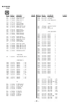
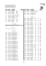
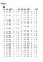
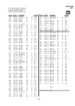
– 47 –
– 46 –
– 48 –
A
1234
5678
9
1
0
1
1
1
2
13
14
15
16
17
18
19
20
21
22
B
C
D
D
E
F
G
H
I
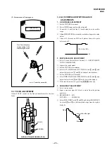
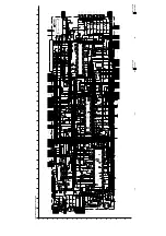
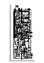
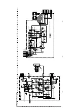
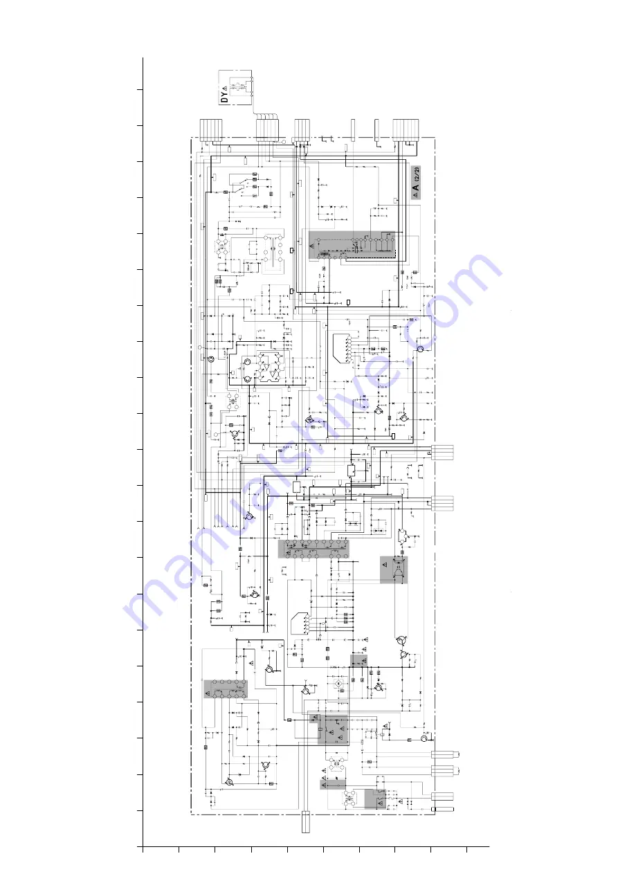
(2) Sc
hematic Dia
gram of A
2/2
boar
d
HV
1
4
2
3
6
5
11
13
9
8
7
FV
SV
10
14
1
2
1
2
3
4
5
1
2
3
1
2
3
4
5
6
1
2
3
4
5
6
7
1
2
3
4
5
6
7
8
1
3
4
7
8
9
10
1
2
1
2
3
4
5
6
1
2
3
4
1
2
1
2
3
4
1
1
2
3
4
-2
1
2
3
4
5
6
7
S
1
2
3
4
1
2
3
4
5
9
8
7
16
15
18
17
14
13
12
10
11
1
1
1
2
3
4
IO
G
IO
G
1
3
4
5
1
2
4
3
1
2
3
S
1
3
4
5
6
8
9
2
10
11
-2
1
2
3
4
C
629
C
635
L508
C5
6
5
C
560
C
527
R5
6
9
C5
4
0
R5
7
8
C5
5
8
C5
4
1
C
566
C
505
C
557
C
529
C5
5
5
R5
6
8
C
516
L515
R5
0
7
SG
5
0
1
C5
6
8
R5
9
7
C5
1
1
R
524
C5
5
3
C5
5
2
Q
506
C
508
R
556
R
523
R
538
R
619
JW
504
R5
5
9
L505
L506
JW
503
L504
JW
52
5
JW
526
C
548
C
562
R6
4
0
R
643
R
649
C5
2
2
C
547
C
509
C
524
R
642
L503
C5
5
9
C
647
C
650
C
652
R
602
R
609
R
610
R
611
R6
1
2
R6
1
6
C
648
R
657
C5
4
6
R5
2
8
R5
2
9
R5
3
5
R5
3
6
R5
4
0
R5
4
1
R
545
R5
4
6
R
547
R5
5
0
R
520
C
551
R
614
C6
2
3
C5
4
9
R5
9
0
FB
6
1
0
R
644
JW
604
JW
605
C
604
C
536
C
649
T6
0
4
R6
0
7
R
Y
601
C
641
C
526
R
608
R
603
C
636
R6
5
9
R
660
R6
4
5
R
651
R
655
R
527
R
V
500
C
646
R
599
R6
1
7
F
B
600
FB6
0
1
F
B
602
F
B
603
F
B
611
C
514
F
B
501
R6
3
6
C
506
FB5
0
2
R5
21
C
517
R5
6
0
L517
C
501
R
504
R
503
C
500
L516
R
502
R5
4
9
R5
6
2
C
519
R5
8
0
C
530
R5
5
2
R
646
R6
5
0
D6
24
D632
D631
D638
D601
D633
IC
503
C5
8
0
C5
8
1
D617
C
583
D519
D527
D5
28
IC603
CN601
C
612
C
611
C6
0
7
C6
0
8
R
648
R
653
R
661
R
530
R
566
R
522
F
B
615
JR
500
JR
501
C
584
R
516
R5
9
1
R5
9
3
R5
9
4
CN600
D513
R
634
CN602
C
654
C
656
R
681
C6
2
0
C6
5
1
D637
D620
D634
D635
D512
D511
D510
D508
D507
D505
R
518
C
564
R6
0
0
R5
3
4
D636
D622
D615
F
600
CN606
CN604
R
637
R
635
F
B
613
C
617
CN
60
7
C
642
F
B
616
S5
0
2
T
501
R
581
R5
3
3
R5
7
0
L518
L501
L514
R5
5
5
R
574
C
544
C
534
R5
6
3
R5
7
2
R5
7
6
Q
512
R5
8
6
R
531
D533
T
600
CN501
CN502
R5
5
1
R5
7
7
D612
C
633
C
644
C6
4
5
JW
06
6
C5
0
3
C5
0
4
C5
0
7
C
510
C5
1
3
C5
2
3
C5
2
8
C5
3
8
C5
3
9
C5
4
3
C5
5
4
C5
6
1
C5
6
3
C
567
C5
7
0
C5
7
2
C
585
C
573
C5
7
4
C
577
C
582
C6
0
0
C
601
C6
0
5
C
606
C6
1
5
C
616
C6
1
9
C6
2
1
C6
2
6
C
627
C
628
C
632
C
638
C
639
C
640
C
655
C
658
CN503
CN504
CN505
CN508
CN509
CN510
CN603
CN609
D509
D517
D
522
D530
D6
09
D613
D614
D6
1
1
D618
D621
D627
D6
29
D6
30
DY
1
F
B
607
F
B
606
JR
502
JW
501
JW
506
JW
507
JW
508
JW
518
JW
606
JW
607
JW
609
JW
610
JW
611
JW
612
JW
614
L502
L507
L510
L51
1
L51
2
L513
L601
D628
D
521
D531
D532
D602
D506
Q
501
Q
502
Q
505
Q6
05
Q6
0
8
R5
0
0
R
501
R
509
R5
0
8
R
506
R5
1
0
R
511
R5
1
5
R
517
R5
1
9
R5
2
6
R
532
R5
3
7
R5
3
9
R
542
R
543
R
548
R
553
R5
5
4
R5
5
8
R
561
R
564
R
565
R5
6
7
R
571
R
573
R5
7
5
R5
7
9
R5
8
2
R5
8
3
R5
8
4
R5
8
5
R5
8
7
R5
8
8
R5
8
9
R5
9
2
R
601
R
613
R
615
R
620
R6
39
R
641
R
647
R
652
R6
5
4
R
680
S5
0
1
T5
0
3
T5
0
4
T
601
VD
R6
00
T5
0
5
R
631
R
630
R
629
R
628
R
626
R6
2
5
R
624
R
623
R
604
D607
D606
D604
D603
C
657
C
614
C
610
C6
0
9
D504
D523
IC502
R
632
D529
D525
D526
C5
7
1
C5
7
9
R
514
R5
1
3
R5
1
2
R
605
R
618
R5
0
5
R5
2
5
R5
9
8
C5
7
6
D6
23
C5
5
6
C
533
C
532
C
518
D520
C5
3
7
C5
3
1
C6
4
3
C
653
C
634
C
630
C
512
C5
8
6
R5
9
5
Q
511
R5
5
7
D625
JW
615
R6
6
2
R
627
Q
601
Q
602
Q
603
D
608
PH
6
0
0
IC
602
IC601
D605
Q
607
Q
604
Q
503
T
603
D518
IC
604
Q6
0
6
Q
507
Q
509
S
600
Q6
0
0
C
603
R6
2
1
R
656
D600
R
Y
600
JW
011
JW
602
JW
603
JW
601
JW
600
C5
0
2
C5
2
1
D616
F
B
605
C6
2
5
C
631
JW
608
R
606
CN605
F
B
608
R
596
T
H
P
600
C
622
C
624
L509
CN507
D534
R
544
C6
0
2
C
613
JW
015
F
B
612
C6
1
8
D610
F
B
604
C
550
R
622
10
:L
H
L
0
8
47
250V
470p
500V
B
330p
0.
33
:MP
S
33
160V
:H
R
220p
500V
B
470
25V
1.
5
:F
P
R
D
10m
H
:DCC
4.
7
:F
P
R
D
470p
500V
B
680
1/
2W
:F
P
R
D
680p
2kV
B
680p
2kV
B
4.
7k
:R
N
330
270k
1/
2W
10k
:L
H
L
0
8
:L
H
L
0
8
:L
H
L08
470p
500V
B
680
3.
3k
1k
100
16V
1.
5k
47
1
2W
:R
S
#
220k
1/
2W
0.
001
CH:
CHI
P
0.
001
CH:
CHI
P
22
4.
7
:F
P
R
D
2.
2k
:CHI
P
10k
:CHI
P
4
7
k
:CHI
P
680
:CHI
P
6.
8
1/
2W
:F
P
R
D
100
10V
:L
H
L
0
8
0.
1
F
:CHI
P
1
100
25V
10k
:R
N
22k
:RN-
CP
220
:RN-
CP
5.
6k
:CHI
P
5.
6k
:CHI
P
4.
7k
:CHI
P
4.
7k
:CHI
P
15k
:CHI
P
15k
:CHI
P
33k
:CHI
P
100k
:CHI
P
470
:CHI
P
68k
:R
N
7.
5M
M
7.
5M
M
1.
5k
ST
B
0.
1
:MP
S
0.
001
B
:CHI
P
330
25V
#
#
#
#
#
#
#
#
#
#
#
#
#
#
#
#
#
#
#
J
W
(5
MM)
4.
7k
0.
0047
B
:CHI
P
DH5
D1
-0
(M
)
680p
500V
B
0.
1
:P
T
22M
1/
2W
470k
:R
N
1k
:CHI
P
10k
:CHI
P
#
#
#
1
0
:CHI
P
#
10
450V
4.
7
22
0.
047
B
:CHI
P
2S
C
3209-
L
H-
DRI
V
E
1.
1U
H
1.
1U
H
1.
1U
H
1.
1U
H
1.
1U
H
0.
047
200V
:P
T
1.
1U
H
15k
3W
:R
S
33
160V
1.
1U
H
JW(1
5M
M)
0.
0033
B
:CHI
P
10k
:CHI
P
#
#
#
#
#
#
#
18k
:R
N
47
820p
500V
B
100k
:RN-
CP
0.
022
2.
2k
:CHI
P
15k
3W
:R
S
22
2W
:R
S
MA
11
1-T
X
E
RC04-
06S
E
E
RC04-
06S
E
D1N20R-
T
R
#
E
R
A
22-
08T
P
3
T
D
A
8172
V.
O
U
T
#
#
#
#
#
G
P
08DP
K
G
23
H
-PO
SI
GP
08
DP
KG
23
H-P
OS
I
L7809CV
2P
:V
H
0.
0047
500V
E
0.
0047
500V
E
0.
0047
500V
E
0.
0047
500V
E
2.
2k
:CHI
P
4.
7k
1W
:R
S
4.
7k
1W
:R
S
J
W
(5
MM)
#
10k
:RN-
CP
1.
1U
H
0
:CHI
P
0
:CHI
P
#
22k
:CHI
P
0.
47
1/
2W
:F
P
R
D
0.
47
1/
2W
:F
P
R
D
0.
47
1/
2W
:F
P
R
D
#
G
P
08DP
K
G
23
V.
BO
O
S
T
8.
2M
1W
2P
:M
IN
I
#
#
#
470p
CH:
CHI
P
470p
CH:
CHI
P
RD6.
8E
S
-T
1
B
1
RD30E
S
-T
1
B
1
M
A
111-
T
X
M
A
111-
T
X
1S
S
355T
E
1S
S
355T
E
1S
S
355T
E
1S
S
355T
E
1S
S
355T
E
1S
S
355T
E
100
0.
1
25V
F
:C
H
IP
56k
0.
22
2W
:R
S
D1NS
4-
T
A
2
F
M
U-
G
26S
#
#
#
3P
:M
IN
I
82k
3W
:R
S
82k
3W
:R
S
1.
1U
H
100p
1kV
#
2200
25V
J
W
(5
MM)
SW
:L
B
HDT
:HDT
4.
7k
:CHI
P
1k
6.
8k
:CHI
P
:E
L0606
:L
H
L
0
8
JW
(5
m
m
)
#
#
#
#
#
#
#
#
#
3.
3k
#
#
#
#
2.
2k
220
3W
:R
S
0.
1
200V
:P
T
0.
01
250V
#
0.
0022
1kV
R
#
#
0.
0047
500V
E
330p
B
330p
CH:
CHI
P
680p
500V
B
0.
0085
2kV
:P
P
0.
039
400V
:P
P
#
0.
0047
200V
:P
T
0.
0033
630V
:P
P
#
0.
82
250V
:P
P
0.
68
250V
:P
P
#
#
0.
033
200V
:P
T
10
160V
0.
15
200V
:P
T
0.
1
25V
B
:CHI
P
0.
1
250V
#
330p
250V
330p
250V
#
0.
022
400V
:P
P
470p
250V
#
680p
500V
B
1000
25V
#
#
0.
1
25V
B
:CHI
P
0.
1
25V
B
:CHI
P
#
0.
1
25V
B
:CHI
P
#
#
3P
:M
IN
I
#
#
#
#
1P
10K
:CHI
P
E
R
C06-
15S
D
AMPER
R
G
P
10G
+
15V
.R
E
C
T
#
A
U
-01Z
-W
S
A
U
-01Z
-W
S
A
U
-01Z
-W
S
RN-
4Z
#
31DQ
06-
F
C
5
#
#
6P
WH
T
:D
Y
1.
1U
H
#
#
5M
M
10M
M
5M
M
5M
M
10M
M
10M
M
10M
M
#
#
#
#
#
10m
H
HL
C
#
1m
mH
:LH
L0
8
1
mmH
:L
H
L
0
8
:L
H
L08
1S
S
119
R
G
P
10G
-15V
.R
E
C
T
1S
S
355T
E
1S
S
355T
E
1S
S
1
19
1S
S
119
#
#
IR
F
614
P
IN-
O
U
T
2S
K2
84
5
2S
C2712
#
#
100
3W
:R
S
68
3W
:R
S
33k
:CHI
P
68
2W
:R
S
100
3W
:R
S
#
#
#
4.
7k
:RN-
CP
#
22k
RN:
CP
#
0
:CHI
P
5.
6k
:F
P
R
D
#
33k
:R
N
33k
:R
N
2.
2k
#
#
10k
:CHI
P
220k
:CHI
P
4.
7k
:R
N
47k
:CHI
P
#
100k
:CHI
P
#
##
6.
8
:F
P
R
D
#
220
2W
:R
S
220
2W
:R
S
#
1.
2k
:F
P
R
D
#
1.
2
1W
:R
S
470
3W
:R
S
0.3
3
2W
:RS
0.
27
2W
:R
S
47
22k
2W
:R
S
#
4.
7
:CHI
P
#
NX
-1
7
4
8
#
LF
T
#
470p
2kV
B
470p
B
RU
-1P
#
#
47k
:CHI
P
10k
:F
P
R
D
470
1/
2W
:F
P
R
D
#
1k
:CHI
P
#
47k
:CHI
P
82k
:CHI
P
100k
:CHI
P
M
A
111
T
F
541M
RG
P
02-
17P
K
RD33E
S
-T
1
B
0.
0022
500V
E
10
10
100
RG
P
10G
PI
N
-O
U
T
RG
P
10G
200V
.R
E
C
T
NJ
M
2903M
-T
E
2
P
IN-
CO
NT
RO
L
0.
1
1/
2W
:R
F
#
#
#
#
#
#
#
#
#
#
120k
:CHI
P
100k
:RN-
CP
56k
0.
1
:P
T
UD
ZT
E-1
71
5B
470
25V
470
25V
470
25V
100
10V
#
220
2.
2
:B
P
100
10V
47
25V
100
16V
33
160V
0.
033
25V
B
:CHI
P
0
:CHI
P
#
2S
D2578-
CA
H-
O
U
T
J
W
(7
.5
MM)
UDZ
S
T
E
-1710B
#
#
6.
8
10W
2S
D2114K
SW
2S
C2712
PR
O
T
EC
T
IO
N
UN2111
SW
IT
C
H
IN
G
R
D
20E
S
B
2
SW
O
N
3171-
R
P
H
OT
O COUP
L
E
R
S
E
-135N
SEN
SO
R
AMP
S
T
R-
F
6654
RE
G
CO
NT
RO
L
D4S
B
60L
A
/C RE
CT
2S
D2144S
RE
LA
Y
DRI
V
E
2S
A
1091R
PR
O
T
EC
T
2S
C2712
PR
O
T
EC
T
SR
T
E
R
D29-
08J
P
IN DA
NP
E
R
L7805CV
5V
RE
G
2S
C2712
S
W
IT
CHI
NG
T
R
AN
SI
ST
O
R
2S
A
1162
PR
O
T
EC
T
2S
C2712
V-PR
O
T
EC
T
SW
IT
C
H
PU
SH
BU
TTO
N
#
#
#
#
#
#
5.
0M
M
10.
0M
M
10.
0M
M
#
#
0.
0015
50V
CH:
CHI
P
220
16V
#
#
#
#
#
#
#
1.
1U
H
5.
6k
3W
:R
S
#
0
:C
H
IP
1.
2
2W
:R
S
0.
1
:P
P
330
450V
7.
5M
M
JW
5M
M
680p
1.
5kV
11E
Q
S
04-
NT
A
B
0U
H
0.
1
100V
:P
T
33
3W
:R
S
EW
AF
C
HP
30V
+B
9V
5V
NS
M
U
T
E
NS
RO
T
VD
-
VD
+
HD
11V
ABL
11
V
7V
ST
-BY
ST
BY 7
V
AU
D
+
VC
C
A
UDI
-G
ND
.B
LK
0426
.B
LK
0213
.B
LK
029C
.B
LK
029B
.B
LK
029A
.B
LK
042D
*
*
E-A3E-A3
+B
200V
C
ABL
H1
H2
-15V
E
DRV-I
N
Vcc
F.B.-
PL
S
Vee
OUT
-P
UT
Vcc(
OUT
)
REF
-V
OL
T
H+
H+
H-
H-
V-
V+
C
N
701
135V
GND
FB
P
AC
IN
AC
IN
DG
C
DG
C
PF
C
PF
C
15V
VD
+
GND
VD
-
15V
NS
ROT
NS
M
U
T
E
T
O
C
O
AT
IN
G
EAR
T
H
TO
H
V
B
L
O
C
K
GN
D
D
S
OC
P/F
B
NC
DG
C C
HK
DG
C C
HK
GND
7V
11V
NS M
UT
E
E
VIN
NC
3D
-VC
C
3D
+V
CC
GN
D
GN
D
GND
15V
VD
+
200V
GN
D
H1
T
O
D
1
BO
AR
D
GN
D
TO
D
G
C
T
O
B3
BO
AR
D
C
N
6205
T
O
D
H
B
O
A
R
D
C
N
3802
C
N
1801
T
O
D
1
BO
AR
D
C
N
2823
C
N
2822
TO
D
Y
DF
GND
TO
F B
O
A
R
D
C
N
4602
TO
D
G
C
H.
DY
H.
DY
V
.DY
V
.DY
POWER SUPPLY,HV,
MICON,Y/C JUNGLE
(
(
T
O
C
3
BO
AR
D
T
O
C
3
BO
AR
D
B
-S
S
S
10217-
ME
.-
A
..2199
15V
15V
15V
15V
15V
15V
15V
15V
15V
15V
135V
135V
135V
135V
135V
135V
135V
135V
135V
135V
135V
135V
15V
15V
15V
15V
15V
15V
200V
200V
200V
200V
9V
9V
9V
9V
9V
9V
9V
9V
9V
9V
9V
30V
30V
30V
30V
30V
9V
9V
9V
11V
11V
11V
11V
7V
7V
7V
7V
7V
7V
-2
.3
0.2
0
17.1
*
*
0
0.5
127.1
119.9
135.4
0
119.8
2.0
0
16
9.8
17
.0
0
0.7
0
0
0
134.0
0
0
0
0.7
0
0
3.6
8.9
6.8
3.0
3.3
0
1.5
3.7
1.1
5.0
0
9.9
1.1
13
.9
-13
.6
-13
.6
-12
.3
13
.7
1.1
*
*
*
*
*
*
9.7
6.8
0
0
0
0.6
1.1
16
0
65.8
-0
.9
14
13
17.1
3.9
3.7
13.4
13.7


