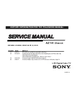
background image

SERVICE MANUAL

LCD Digital Color TV

AZ1-H 

Chassis

9-888-349-04

Version  Date 

Subject

1.0            8/3/2010 

No revisions or updates  are applicable at this time. 

2.0 

8/11/2010 

Updated Special Handling Instructions when Replacing the LCD Panel Assembly.  


Added Wire Dressing Diagrams.  


Added White Balance Adjustments.  Reissue entire manual. 

3.0 

9/30/2010 

Corrected Support Belt Kit PN. Replaced page 20. 

4.0 

2/8/2011 

Corrected disassembly instructions for LCD Panel removal. Replaced page 16.

ORIGINAL MANUAL ISSUE DATE: 8/2010

HISTORY INFORMATION FOR THE FOLLOWING MANUAL:

Summary of Contents for BRAVIA KDL-46NX810

Page 1: ...pecial Handling Instructions when Replacing the LCD PanelAssembly Added Wire Dressing Diagrams Added White BalanceAdjustments Reissue entire manual 3 0 9 30 2010 Corrected Support Belt Kit PN Replaced page 20 4 0 2 8 2011 Corrected disassembly instructions for LCD Panel removal Replaced page 16 ORIGINAL MANUAL ISSUE DATE 8 2010 HISTORY INFORMATION FOR THE FOLLOWING MANUAL ...

Page 2: ...SERVICE MANUAL LCD Digital Color TV AZ1 H Chassis 9 888 349 04 SelfDiagnosis Supported model ...

Page 3: ...ER DESTINATION MODEL COMMANDER DESTINATION 9 888 349 04 KDL 46NX810 RM YD036 US KDL 46NX810 RM YD051 CND KDL 55NX810 RM YD036 US KDL 55NX810 RM YD051 CND KDL 55NX811 RM YD051 MX KDL 60NX810 RM YD036 US KDL 60NX810 RM YD051 CND ...

Page 4: ... 15 1 3 G9B G10 G11 Power Boards BUHT Board HLT Board Wireless LAN Card and LCD Panel Assembly Removal 16 1 3 1 KDL 46NX810 55NX810 55NX811 Only 16 1 3 2 KDL 60NX810 Only 17 1 4 Cleaning the LCD Panel Assembly 18 1 5 Screw Legend 18 1 6 Connectors 19 1 6 1 KDL 46NX810 55NX810 55NX811 Only 19 1 6 2 KDL 60NX810 Only 19 1 7 Accessories and Packing 20 1 8 Miscellaneous 20 1 9 Remote Commander 20 1 10 ...

Page 5: ... 26 2 2 1 Updating the Software 26 2 2 2 Selecting the Model 27 2 2 3 Setting the Destination 28 2 2 4 Resetting the Data Value in the Panel Engine Micro 29 2 2 5 Verifying the Emitter Output Level 32 2 2 6 Verifying the Model and Panel Information 33 2 2 7 Reconnecting All Cables 33 2 3 White Balance Adjustments 34 2 4 Resetting the TV to Factory Condition 35 2 4 1 Resetting the TV to Factory Con...

Page 6: ...ter Entertainment Inc DLNA the DLNA Logo and DLNA CERTIFIED are trademarks service marks or certification marks of the Digital Living Network Alliance Your BRAVIA TV is ENERGY STAR qualified in the Home mode It meets strict energy efficiency guidelines set by the U S Environmental Protection Agency and Department of Energy ENERGY STAR is a joint program of these government agencies designed to pro...

Page 7: ...s 54 6 inches 55 class r o h s t o d 0 2 9 1 n o i t u l o s e r y a l p s i D izontal 1 080 lines vertical Speaker Full range mm inches Woofer mm inches 20 70 4 13 16 2 7 8 4 Φ 60 1 Φ 2 3 8 1 Dimensions with stand mm inches 1 400 865 303 55 1 8 34 1 8 12 1 276 800 323 50 1 4 31 1 2 12 3 4 1 083 690 270 42 3 4 27 1 4 10 3 4 withoutstand mm inches 1 400 836 45 55 1 8 33 1 7 8 1 276 770 32 50 1 4 30...

Page 8: ...sis The chassis of this receiver is directly connected to the AC power line SAFETY RELATED COMPONENT WARNING Components identified by shading and mark on the exploded views are critical for safe operation Replace all components with Sony parts whose part numbers appear as shown in this manual or in supplements published by Sony It is essential that all critical parts be replaced only with the part...

Page 9: ...cution provenant d un chássis sous tension un transformateur d isolement doit etre utilisé lors de tout dépannage Le chássis de ce récepteur est directement raccordé à l alimentation du secteur ATTENTION AUX COMPOSANTS RELATIFS A LA SECURITE Les composants identifies par une trame et par une marque sur les schemas de principe les vues explosees et les listes de pieces sont d une importance critiqu...

Page 10: ... R If the glass needs additional cleaning slightly moisten the cloth with a diluted mild soap or mild detergent solution or use a compressed air duster spray can type R After replacing the Glass Assembly verify there are no dark spots or finger prints visible on the screen CAUTION W Do Not use paper towels any type of abrasive pad rags rubber or vinyl materials to clean the screen Using these mate...

Page 11: ...oving the boards and connectors note where the frame is on the panel See Figure 1 2 Lift the LCD Panel Assembly by holding the top and bottom of the panel approximately 200mm from the edge with your palms on the back of the panel See Figure 2 CAUTION Lifting or holding the panel at the corners may damage the panel 3 Use the same method when taking the replacement panel out of the carton See Figure...

Page 12: ...n areas of high humidity for an extended period of time 4 Do not expose the LCD Panel Asembly to direct sunlight 5 Avoid contact with water It may cause a short circuit within the module 6 Disconnect the AC power when replacing the backlight or inverter circuit High voltage occurs at the inverter circuit at 650Vrms 7 Always clean the LCD Panel Asembly with a soft cloth material 8 Use care when han...

Page 13: ...ain that you have replaced all the insulators 4 Look for unauthorized replacement parts particularly transistors that were installed during a previous repair Point them out to the customer and recommend their replacement 5 Look for parts which though functioning show obvious signs of deterioration Point them out to the customer and recommend their replacement 6 Check the line cords for cracks and ...

Page 14: ... The Simpson s 250 and Sanwa SH 63TRD are examples of passive VOMs that are suitable Nearly all battery operated digital multimeters that have a 2 VAC range are suitable see Figure A HOW TO FIND A GOOD EARTH GROUND A cold water pipe is a guaranteed earth ground the cover plate retaining screw on most AC outlet boxes is also at earth ground If the retaining screw is to be used as your earth ground ...

Page 15: ... the LED will identify the first of the problem areas Result for all of the following diagnostic items are displayed on screen If the screen displays a 0 no error has occurred Diagnostic Item Diagnostic Item Description Number of times Standby LED blinks Possible Location RGB_SEN RGB Sensor ACK Error NA NA MAIN_POWER Main Power Over Voltage Protection 2 G9B Power Board KDL 46NX810 55NX810 55NX811 ...

Page 16: ...KDL 46NX810 55NX810 55NX811 60NX810 11 SELF DIAGNOSIS FUNCTIONS STANDBY LED FLASH COUNT Ambient Sensor IR Infrared Receiver Picture Off Timer LED Standby LED Power LED 0 5 0 5 3 0 5 0 5 3 ...

Page 17: ...ode Volume Total operation time by hour MAX 65535 Boot count MAX 65535 Panel operation time by hour MAX 65535 Total operation time by hour MAX 65535 Boot count MAX 65535 Panel operation time by hour MAX 65535 0501210811 0412311234 0311111825 00 00 00 00 00 002 MAIN_POWE 003 DC_ALERT1 003 AUD_PROT 004 BALANCER 005 HFR_ERR 005 P_ID_ERR 12345 00333 06789 12345 00333 06789 00 003 DTT_WDT 00 005 TCON_E...

Page 18: ...completed the repairs to be sure you have cleared the result display to 0 1 To clear the Error history and Error count Press the Channel 8 Channel 0 2 To clear the Panel operation time Press the Channel 7 Channel 0 EXITING THE SELF CHECK DIAGNOSTIC SCREEN 1 To exit the Self Diagnostic screen turn off the power to the TV by pressing the POWER button on the remote or the POWER button on the TV SELF ...

Page 19: ... the panel For more information Refer to Special Handling Instructions When Replacing the LCD Panel Assembly on page 6 A Remove screws from Table Top Stand Assembly 3 from KDL 46NX810 55NX810 55NX811 Only 5 from KDL 60NX810 Only B Lift up TV set to detach from Table Top Stand Assembly REF NO PART NO DESCRIPTION ASSEMBLY INCLUDES REF NO PART NO DESCRIPTION ASSEMBLY INCLUDES C Gently place the LCD P...

Page 20: ...d lift up right side Speaker to detach from Bezel Bottom H Remove 2 screws to detach Bottom Frame from LCD Panel Assembly I Disconnect 1 connector and lift up left side Speaker to detach from Bezel Bottom J Remove screws from Bezel Bottom to detach from LCD Panel Assembly 3 from KDL 46NX810 Only 5 from KDL 55NX810 55NX811 60NX810 Only K Remove 2 screws from Antennas to detach from LCD Panel Assemb...

Page 21: ...Panel Assembly on page 6 Note The Tape PWB H Side Jack Label Terminal Label Insulation Sheet G and Attachment GL pieces are not included with the LCD Panel Assembly and must be replaced when replacing the LCD Panel Assembly A Remove 2 screws from Wireless LAN Card to detach from LCD Panel Assembly B Gently peel off HLT Board and Disconnect 1 connector to detach from LCD Panel Assembly C Gently pee...

Page 22: ...l to detach from LCD Panel Assembly B Gently peel off Side Jack Label to detach from LCD Panel Assembly C Remove 2 screws from Wireless LAN Card to detach from LCD Panel Assembly D Gently peel off HLT Board and Disconnect 1 connector to detach from LCD Panel Assembly E Gently peel off Tape PWB H to detach from HLT Board F Remove 9 screws from BUHT Board to detach from LCD Panel Assembly G Release ...

Page 23: ...e instruction provided on the package Never use strong solvents such as a thinner alcohol or benzine for cleaning Periodic vacuuming of the ventilation openings is recommended to ensure the proper ventilation 1 5 SCREW LEGEND P N DESCRIPTION REMARKS TOTAL 4 167 019 11 SCREW PSW M3X8 RC 11 AC CVR 1 SP BOX to PNL 3 15 4 159 298 01 SCREW PSW M4X10 RC to BTM FRM 2 BTM FRM to PNL 2 4 3 452 815 01 SCREW...

Page 24: ...TOR ASSEMBLY 3P 254 1 910 101 87 CONNECTOR ASSEMBLY 14P 255 1 910 101 89 CONNECTOR ASSEMBLY 5P 1 6 CONNECTORS CN6150 46 CN6403 55 CN6151 CN8500 CN6003 G9B CN6002 CN2602 CN2600 CN5500 CN3800 CN4300 BUHT SP SP HLT WIFI ILLUMINATION MODULE SWITCH UNIT POWER SWITCH TCON SP 201 204 203 202 207 206 205 REF NO PART NO DESCRIPTION ASSEMBLY INCLUDES REF NO PART NO DESCRIPTION ASSEMBLY INCLUDES 1 6 2 KDL 60...

Page 25: ... INSTRUCTION KDL 55NX811 ONLY 4 198 235 51 MANUAL INSTRUCTION KDL 55NX811 ONLY 1 838 333 11 POWER SUPPLY CORD WITH CONN 4 208 536 21 SUPPLEMENT STAND INSTALLATION 1 8 MISCELLANEOUS X 2548 310 1 BAG SCREW ASSEMBLY E 4 259 974 01 POST PWB MINI 4 100 136 01 SHEET CORE C KDL 46NX810 55NX810 55NX811 ONLY 4 188 689 01 SHEET THERMAL B2 4 259 997 01 SHEET THERMAL B SMALL X 2549 230 1 SUPPORT BELT KIT 7 60...

Page 26: ...KDL 46NX810 55NX810 55NX811 60NX810 21 DISASSEMBLY PART NUMBER INFORMATION 1 10 WIRE DRESSING DIAGRAMS 1 10 1 KDL 46NX810 ONLY ...

Page 27: ...KDL 46NX810 55NX810 55NX811 60NX810 22 DISASSEMBLY PART NUMBER INFORMATION 1 10 2 KDL 55NX810 55NX811 ONLY ...

Page 28: ...KDL 46NX810 55NX810 55NX811 60NX810 23 DISASSEMBLY PART NUMBER INFORMATION 1 10 3 KDL 60NX810 ONLY ...

Page 29: ...ond of each other DISPLAY Channel 5 Volume POWER POWER Onscreen cursor and select button DISPLAY RM YD036 5 VOLUME DIGITAL SERVICE 001 OP 000 VERS MAIN SUB DM1 301J00AA SM1 010W00AA M2 105C SB1 000W00AA DD1 016J00AA SD1 010W00AA DM1 301J00AA RF01 05 WP00 521J00AA ID1C117081 ID1C117081 LTY320AB01 PID04020000 WF 2 0 0 99 BEM WF 0B BM1 012W00LU Camera FW BB1 000W00LU Camera FW BD1 011J46LUX Sample Se...

Page 30: ...IN SUB DM1 301J00AA SM1 010W00AA M2 105C SB1 000W00AA DD1 016J00AA SD1 010W00AA DM1 301J00AA RF01 05 WP00 521J00AA ID1C117081 ID1C117081 LTY320AB01 PID04020000 WF 2 0 0 99 BEM WF 0B BM1 012W00LU Camera FW BB1 000W00LU Camera FW BD1 011J46LUX Sample Digital Service Menu press or JUMP OPTIONS CHASSIS 000 CXD2813R 000 H_DET_NOSIG_CNT 1 Within each Service Menu are Categories and data information CHAS...

Page 31: ... 0 to WRITE Save the changes 8 To exit service mode press HOME or turn the TV power off 2 2 ADJUSTMENTS AFTER REPLACING THE BUHT BOARD OR LCD PANEL ASSEMBLY The following procedures must be completed after replacing the BUHT Board or the LCD Panel Assembly þ Update the TV to the latest software version þ Select the Model þ Select the Destination þ Reset the Data Value in the Panel Engine Micro þ V...

Page 32: ...e Commander DIGITAL SERVICE 001 OP 000 VERS MAIN SUB DM1 301J00AA SM1 010W00AA M2 105C SB1 000W00AA DD1 016J00AA SD1 010W00AA DM1 301J00AA RF01 05 WP00 521J00AA ID1C117081 ID1C117081 LTY320AB01 PID04020000 WF 2 0 0 99 BEM WF 0B BM1 012W00LU Camera FW BB1 000W00LU Camera FW BD1 011J46LUX 4 Press 2 to move to the 002 MODEL Next category DIGITAL SERVICE 002 MODEL 000 SEG 04 2a 1 5 5 Using the table p...

Page 33: ...s 3 to increase the data value or 6 to decrease the data value to select the destination of the TV GROUP DESTINATION CODE DATA VALUE DESTINATION UC 3 US CND LTN D 16 MX LATIN AMERICA UC grp DIGITAL SERVICE 002 MODEL 001 DEST 03 UC UC grp Data Value Destination CAUTION Verify the DESTINATION is set correctly before proceeding to the next step If another destination Data Value is selected it may pos...

Page 34: ...ONS on the Remote Commander until the PEM Service Menu displays PEM SERVICE 000 VERSION MAIN BOOT DATA NLD NLD DATA QDL NVM 33 LD1 00 37 1 0018W00LA 1 002W00LA 1 017WA46LF 12 Press 2 to move to the 001 DL category PEM SERVICE 001 000 DL DLCC 0 13 Press 1 to move to the 001 PRETEND_ID item PEM SERVICE 001 001 DL PRETEND_ID 0 14 Press 3 to increase the data value to 1 PEM SERVICE 001 001 DL PRETEND_...

Page 35: ...tegory displays PEM SERVICE 004 000 TCON_CHANGED DATA_TRANS_SET 0 17 For the DATA_TRANS_SET item press 3 to increase the data value to 1 PEM SERVICE 004 000 TCON_CHANGED DATA_TRANS_SET 1 Data Value 18 Press 1 until the 001 DATA_TRANS_EXE item displays PEM SERVICE 004 001 TCON_CHANGED DATA_TRANS_EXE 0 ...

Page 36: ... Warning Message Displays After the update is complete the data value changes back to 0 and a message indicating the data transter was successful displays PEM SERVICE 004 001 TCON_CHANGED DATA_TRANS_EXE 0 DATA TRANSFER SUCCESS Data Value Confirmation Message Displays 20 Press 2 until the 005 LDRV_CHANGED item displays PEM SERVICE 005 000 LDRV_CHANGED DATA_TRANS_SET 0 21 For the DATA_TRANS_SET item...

Page 37: ...omplete the data value changes back to 0 and a message indicating the data transter was successful displays 24 Proceed to Verifying the Emitter Output Level 2 2 5 VERIFYING THE EMITTER OUTPUT LEVEL If necessary the emitter LED output level can be increased or decreased 25 Press 2 until the 009 3D category displays PEM SERVICE 009 000 EMIT_STR 3D 0 Default Data Value 26 Using the table below press ...

Page 38: ...1J00AA ID1C117081 ID 86d731ae PID0caa0000 WF 2 0 0 99 BEM WF 0B BM1 012W00LU Camera FW BB1 000W00LU Camera FW BD1 011J46LUX xxxxxxxxxxxxxx Model ID Product ID 4 Using the table verify the Model ID and the Product ID match the information in the Service Menu Model Name Model ID Product ID KDL 46NX810 86d731ae 0caa0000 KDL 46NX810 86d731c2 0caa0000 KDL 55NX810 86d731af 0caa0000 KDL 55NX810 86d731c3 ...

Page 39: ...displays NOTE There are 4 Service Menus for these models DIGITAL CHASSIS SUB and PEM DIGITAL SERVICE 001 OP 000 VERS MAIN SUB DM1 301J00AA SM1 010W00AA M2 105C SB1 000W00AA DD1 016J00AA SD1 010W00AA DM1 301J00AA RF01 05 WP00 521J00AA ID1C117081 ID1C117081 LTY320AB01 PID04020000 WF 2 0 0 99 BEM WF 0B BM1 012W00LU Camera FW BB1 000W00LU Camera FW BD1 011J46LUX 4 Press JUMP or OPTIONS on the Remote C...

Page 40: ...e on the Remote Commander press the POWER button on the TV Switch Unit of the set The set restarts and displays the Initial Setup screen This may take several minutes 2 4 1 RESETTING THE TV TO FACTORY CONDITION USING SERVICE MODE 1 TV must be in Standby Mode POWER off 2 Press the following buttons on the Remote Commander within a second of each other DISPLAY Channel 5 Volume POWER 3 If necessary p...

Page 41: ...KDL 46NX810 55NX810 55NX811 60NX810 36 SEC 3 DIAGRAMS 3 1 CIRCUIT BOARDS LOCATION G9B KDL 46NX810 55NX810 55NX811 ONLY G10 KDL 60NX810 ONLY G11 KDL 60NX810 ONLY WIRELESS LAN CARD SWITCH UNIT HLT BUHT ...

Page 42: ...UT_L R HP LINEOUT_L R TVOUT_L R M_SPDIF_OUT HDMIB_TMDS DCCB_I2C HDMIC_TMDS DCCC_I2C DCCD_I2C ARC Audio SW DAC AMP Inlay D Amp TAS5707 OneNAND 1Gb DDR2 1Gb x2 EMMA3TH2 DEBUG I F UART2_TXD RXD Power UART0_TXD RXD UART1_TXD RXD LVDS VIDEO Mimas MB91F313 SPI LVDS EEP Temp Sensor PANEL_SCL SDA RF_TXD RXD DEVICE_SCL SDA TV_TXD RXD REM_TXD RXD MS H Board Tcon Board ASSIST SP D Amp TAS5707 WiFi USB2 0_2 U...

Page 43: ...n Sony Technology Center Technical Services Service Promotion Department 9 888 349 04 English 2010HJ74WEB 1 Printed in USA 2010 8 is a trademark of Sony Electronics Reproduction in whole or part without written permission is prohibited All rights reserved ...

Page 44: ...RM YD051 MX KDL 60NX810 RM YD036 US KDL 60NX810 RM YD051 CND LEVEL 3 CONFIDENTIAL HISTORY INFORMATION FOR THE FOLLOWING MANUAL ORIGINAL MANUAL ISSUE DATE 8 2010 REVISION DATE SUBJECT 8 2010 No revisions or updates are applicable at this time 8 11 2010 Revised instructions for Special Handling Instructions When Replacing the LCD Panel Assembly Replaced page 5 CONFIDENTIAL ELECTRICAL SERVICE MANUAL ...

Page 45: ... of 18 18 BUHT Board Schematic Diagram 7 of 18 19 BUHT Board Schematic Diagram 8 of 18 20 BUHT Board Schematic Diagram 9 of 18 21 BUHT Board Schematic Diagram 10 of 18 22 BUHT Board Schematic Diagram 11 of 18 23 BUHT Board Schematic Diagram 12 of 18 24 BUHT Board Schematic Diagram 13 of 18 25 BUHT Board Schematic Diagram 14 of 18 26 BUHT Board Schematic Diagram 15 of 18 27 BUHT Board Schematic Dia...

Page 46: ...ant for safety and to avoid damage Warning An isolation transformer should be used during any service to avoid possible shock hazard because of live chassis The chassis of this receiver is directly connected to the ac power line Safety related component warning Components identified by shading and mark on the schematic diagrams exploded views and in the parts list are critical for safe operation R...

Page 47: ...ve any dust or dirt particles R If the glass needs additional cleaning slightly moisten the cloth with a diluted mild soap or mild detergent solution or use a compressed air duster spray can type R After replacing the Glass Assembly verify there are no dark spots or finger prints visible on the screen CAUTION W Do Not use paper towels any type of abrasive pad rags rubber or vinyl materials to clea...

Page 48: ...ter removing the boards and connectors note where the frame is on the panel See Figure 1 2 Lift the LCD Panel Assembly by holding the top and bottom of the panel approximately 200mm from the edge with your palms on the back of the panel See Figure 2 CAUTION Lifting or holding the panel at the corners may damage the panel 3 Use the same method when taking the replacement panel out of the carton See...

Page 49: ... alerte Afin d eviter tout risque d electrocution provenant d un chássis sous tension un transformateur d isolement doit etre utilisé lors de tout dépannage Le chássis de ce récepteur est directement raccordé à l alimentation du secteur Attention aux composants relatifs a la securite Les composants identifies par une trame et par une marque sur les schemas de principe les vues explosees et les lis...

Page 50: ...with any sharp objects Ú do not leave the module in high temperatures or in areas of high humidity for an extended period of time Ú do not expose the LCD Panel Assembly to direct sunlight Ú avoid contact with water It may cause a short circuit within the module Ú disconnect the AC adapter when replacing the backlight CCFL or inverter circuit High voltage occurs at the inverter circuit at 650Vrms Ú...

Page 51: ... the following part numbers Due to the higher melting point of Lead Free Solder the soldering iron tip temperature needs to be set to 370 degrees centigrade This requires soldering equipment capable of accurate temperature control coupled with a good heat recovery characteristics For more information on the use of Lead Free Solder please refer to http www sony training com r e b m u n t r a P r e ...

Page 52: ...ed 0 5 mA 500 microamperes Leakage current can be measured by any one of three methods 1 A commercial leakage tester such as the Simpson 229 or RCA WT 540A Follow the manufacturers instructions to use these instructions 2 A battery operated AC milliampmeter The Data Precision 245 digital multimeter is suitable for this job 3 Measuring the voltage drop across a resistor by means of a VOM or battery...

Page 53: ...mation Specific instructions must be adhered to whenever these components are repaired and or replaced See Appendix A Encryption Key Components in the back of this manual All capacitors are in μF unless otherwise noted pF μμF 50WV or less are not indicated except for electrolytics and tantalums All electrolytics are in 50V unless otherwise specified All resistors are in ohms k 1000 M 1000k Indicat...

Page 54: ...athode Common Cathode Cathode Common Cathode Cathode Common Common Common Common Cathode Anode Base Emitter Collector Base Emitter Collector Drain Gate Gate Drain Device Printed symbol Terminal name Circuit Terminal name of semiconductors in silk screen printed circuit Anode Anode Anode Cathode Anode Anode Cathode Transistor FET Transistor FET Emitter Collector Base Transistor Source Gate Drain Ca...

Page 55: ...CL1 SDA1 MUXOUT_L R HP LINEOUT_L R TVOUT_L R M_SPDIF_OUT HDMIB_TMDS DCCB_I2C HDMIC_TMDS DCCC_I2C DCCD_I2C ARC Audio SW DAC AMP Inlay D Amp TAS5707 OneNAND 1Gb DDR2 1Gb x2 EMMA3TH2 DEBUG I F UART2_TXD RXD Power UART0_TXD RXD UART1_TXD RXD LVDS VIDEO Mimas MB91F313 SPI LVDS EEP Temp Sensor PANEL_SCL SDA RF_TXD RXD DEVICE_SCL SDA TV_TXD RXD REM_TXD RXD MS H Board Tcon Board ASSIST SP D Amp TAS5707 Wi...

Page 56: ..._DATA M_UART0_RX 47 RB9013 2 1 4 3 6 5 8 7 D 3 3V X_M_WDT 1 16W CHIP 5 10k R9026 10k R9006 50V C9002 5p R9016 10k M_SDA1 1 2 32 768MHz 181439211 X9001 50V C9004 5p GND_D 1005 1 16W R9008 10k M_DIMMER 10k RB9014 2 1 4 3 6 5 8 7 47 RB9006 2 1 4 3 6 5 8 7 GND_D 1 16W 47 R9017 M_MSCLK_CLK D 3 3V 220 R9014 CL9022 M_PCI_CLK_33M M_UART1_RX M_UART2_RX M_MSDATA0 M_SCL0 M_SCL1 DOWNLOAD_CLK DOWNLOAD_CS X_U_B...

Page 57: ...ADD16 AJ8 RADD17 AH8 RADD18 AL7 RADD19 AK7 RADD20 AJ7 RADD21 AH7 RADD22 AK6 RADD23 AG10 RADD24 AJ6 RADD25 AG8 RDQ0 AN7 RDQ1 AN6 RDQ2 AM6 RDQ3 AL6 RDQ4 AN5 RDQ5 AM5 RDQ6 AL5 RDQ7 AN4 RDQ8 AM4 RDQ9 AK5 RDQ10 AN3 RDQ11 AM3 RDQ12 AJ5 RDQ13 AL4 RDQ14 AM2 RDQ15 AL3 ROEB AL2 RWEB AL1 RCSB0 AL11 RCSB1 AN10 RCSB2 AM10 RCSB3 AN9 NALE AL9 NCLE AL8 NOEB AM8 NWEB AN8 NRBB AM11 10k R9268 M_RADD 10k R9284 X_M_FE...

Page 58: ...D P30 MGND P29 MGND P28 MGND P27 MGND P26 MGND P25 MGND R27 MGND T28 MGND T26 MGND U29 MGND V31 MGND V30 MGND V26 MGND W33 MGND W32 MGND W25 MGND Y26 MGND AA27 MGND AB28 MGND AB26 MGND AC29 MGND AD31 MGND AD30 MGND AD26 MGND AE33 MGND AE32 MGND AJ32 UMALVDD AB25 UMALVDD AA25 UMAHVDD U25 UMAHVDD T25 UMVREF1 V25 UMVREF0 AC25 UMCKERSTB AB29 UMDQ0 AF30 UMDQ1 AG29 UMDQ2 AE26 UMDQ3 AF28 UMDQ4 AG28 UMDQ5...

Page 59: ...10 G12 VADDVDD G10 VDFDGND3 B14 VDFAGND3 B13 VADDGND G11 VDFPGND1 J15 VDPHEDGND H16 VADIOGND10 H12 AVI0VCOM D15 AVI0VRB F15 AVI0VRT G15 AVI0AVDD18 E14 AVI0AVDD18 G14 AVI0AGND A15 AVI0AGND B15 AVI0AGND C15 AVI0AGND D16 AVI0AGND H14 AVI1AVDD18 D10 AVI1AVDD18 F10 AVI1AGND E11 AVI1AGND E9 AVI2AVDD18 A10 AVI2AVDD18 B10 AVI2AGND C9 AVI2AGND F16 AVI3AVDD18 A12 AVI3AVDD18 C12 AVI3AVDD18 D12 AVI3AVDD18 F12...

Page 60: ...008 6B 008 10C M_EAI0_LRCK_CLK 008 6B 008 10C M_EAI0_BCK_CLK 008 7E 008 10C M_EAI0_LRCK_CLK 008 7E 008 10C M_ARC_OUT_HSS 021 13F 021 13F M_S_DATA_HSS 031 2F M_S_LRCK_CLK 031 2F M_S_BCK_CLK 031 2F 47 RB4517 2 1 4 3 6 5 8 7 100ohm FB4502 M_AUDIO_GPIO3 003 7D 008 8G M_AUDIO_GPIO3 003 7D 008 7G 74AHC1G08GW 125 IC4503 1 IN_B 2 IN_A 3 GND 4 OUT_Y 5 VCC 16V 0 1 X7R C4523 D 3 3V X_HDMI_MUTE 031 2G X_M_AUD...

Page 61: ...GND N21 PLSVGND P20 PLSBVDD P13 PLS0VDD AA16 PLLGVDD H25 PLSBGND N13 PLS0GND Y16 PLLGGND J25 IOVDD H24 IOVDD H17 IOVDD H11 IOVDD J23 IOVDD J21 IOVDD J19 IOVDD J14 IOVDD J12 IOVDD J10 IOVDD L25 IOVDD K9 IOVDD L7 IOVDD M25 IOVDD N9 IOVDD N7 IOVDD R7 IOVDD U7 IOVDD V9 IOVDD W8 IOVDD Y9 IOVDD AA8 IOVDD AB9 IOVDD AC8 IOVDD AD9 IOVDD AE18 IOVDD AE16 IOVDD AE14 IOVDD AE12 IOVDD AE10 IOVDD AE8 IOVDD AF17 ...

Page 62: ... 0 1 C9902 X7R GND_D 1005 16V 0 1 C9916 M_LVDS_VS 033 11G GND_D 1005 16V C9912 X7R 0 1 1005 25V 0 01 X7R C9901 LTVDD Graphics IC9002 MC 10152F1 RNB A LTGEDP0 J30 LTGEDN0 J31 LTGEDP1 H31 LTGEDN1 H30 LTGEDP2 G29 LTGEDN2 H29 LTGEDP3 F30 LTGEDN3 F31 LTGEDP4 D31 LTGEDN4 E31 LTGECP G30 LTGECN G31 LTGODP0 J32 LTGODN0 J33 LTGODP1 H32 LTGODN1 H33 LTGODP2 G32 LTGODN2 G33 LTGODP3 E32 LTGODN3 E33 LTGODP4 D32 ...

Page 63: ...1 TU_DEM 3 3V_SW TU_DEM 2 5V_SW GND_D 1005 CHIP R1066 0 1005 CHIP R1067 0 8 7 6 5 4 3 2 1 875927858 NJM4558V TE2 IC1009 AOUT A IN A IN GND B IN B IN BOUT VCC 1 16W CHIP 5 4 7k R1085 1 16W CHIP 5 10k R1006 1 16W RN CP 0 5 10k R1086 1 16W CHIP 5 3 3k R1087 1 16W CHIP 5 10k R1088 1 16W CHIP 5 4 7k R1089 1005 50V 47p CH C1095 1608 16V 111481311 1 X7R C1101 1005 50V 0 001 X7R C1100 1005 50V 47p CH C110...

Page 64: ...V1_CV GND_D GND_D C2902 1000p 2 1 4 3 1M RB2902 2 1 4 3 6 5 8 7 1k RB2904 2 1 4 3 6 5 8 7 1M RB2903 2 1 4 3 6 5 8 7 C2900 1000p 2 1 4 3 YEL WHT RED RED WHT J2900 4 5 6 7 8 1 2 3 9 10 11 12 GND_D 1608 10V 1 X7R C2105 VD2102 GND_D 50V X7R C2100 1000p 2 1 4 3 1 2 ASW_IN3_L RED WHT RED GRN BLU J2101 4 5 6 7 8 1 2 3 9 10 11 12 13 1608 10V 1 X7R C2104 VSW_C1PR C2PR C3PR D1_DET GND_D VD2105 VD2106 1k RB2...

Page 65: ...3X1N 24 R3X1P 25 R3X2N 26 R3X2P 27 VCC33 28 RSVDL 29 DSDA0 30 DSCL0 31 CBUS_HPD0 32 R0PWR5V 33 DSDA1 34 DSCL1 37 MICOM_VCC33 38 SBVCC33 39 DSDA2 40 DSCL2 41 CBUS_HPD2 42 R2PWR5V 43 DSDA3 44 DSCL3 45 CBUS_HPD3 46 R3PWR5V 47 DSDA4 48 DSCL4 49 R4PWR5V 50 CEC_A 51 CEC_D 55 TPWR_CI2CA 56 TX2P 57 TX2N 58 TX1P 59 TX1N 60 TX0P 61 TX0N 62 TXCP 63 TXCN 64 VCC33 65 R0XCN 66 R0XCP 67 R0X0N 68 R0X0P 18 R2X2P 3...

Page 66: ...19 HPD 20 20P CN2260 1 D2 2 E 3 D2 4 D1 5 E 6 D1 7 D0 8 E 9 DO 10 CLK 11 E 12 CLK 13 CEC 14 ARC 15 DDC CLK 16 DDC DAT 17 E 18 DDC 5V 19 HPD 20 ARC_OUT_HSS 100 R2286 100 R2285 D 3 3V X_HDMIA_DET X_HDMIB_DET R2288 100 100 R2287 X_HDMIC_DET RB2265 10k 47K RB2262 2 1 4 3 6 5 8 7 47K RB2260 2 1 4 3 6 5 8 7 47K RB2261 2 1 4 3 6 5 8 7 47K RB2263 2 1 4 3 6 5 8 7 HDMI_CEC_IN OUT D2200 MA2SD320G8S0 1005 16V...

Page 67: ... 4 3 6 5 8 7 GND_D C2307 0 1 1005 16V X7R GND_D GND_D 1 16W CHIP 5 R2300 1k CL2303 GND_D D 3 3V M_PC_V 007 6E PC_DDC_SCL PC_DDC_SDA PC_DDC 5V M_PC_H 007 6E 1608 10V 1 X7R C2303 ASW_IN4_L 031 2J VD2301 1608 10V 1 X7R C2302 1 2 GND_D ASW_IN4_R 031 2J C2300 1000p 2 1 4 3 1M RB2300 2 1 4 3 6 5 8 7 VD2300 8 7 6 5 4 3 2 1 S 24CS02AFJ TB G IC2300 M_PC_G M_PC_B M_PC_R PC_RGB 007 2C CN2300 1 2 3 4 5 6 7 8 ...

Page 68: ...X_U_BOOT_RST 024 2F 002 2F 002 3C 002 4B 10p C2442 125027181 6 49k R2413 KSZ8041RNL IC2400 1 GND 2 VDDPLL_1 8 3 VDDA_3 3 4 RX 5 RX 6 TX 7 TX 8 XO 9 X I 10 REXT 11 MDIO 12 MDC 13 PHYAD0 14 PHYAD1 15 RXD1 PHYAD2 16 RXD0 DUPLEX 17 VDDIO_3 3V 18 CRS_DV CONFIG2 19 REF_CLK 20 RX_ER ISO 21 INTRP 22 NC 23 TX_EN 24 TXD0 25 TXD1 26 NC 27 NC 28 CONFIG0 RMII mode 29 CONFIG1 30 LED0 NWAYEN 31 LED1 SPEED 32 RST...

Page 69: ...ODD2_P 028 3E PANEL_ODD_CLK_P 028 3E PANEL_ODD_CLK_N 028 3E PANEL_ODD1_P 028 3E PANEL_ODD1_N 028 3E PANEL_ODD0_P 028 3E PANEL_ODD0_N 028 3E R2595 10k GND_D JL2564 GND_D M_DIMMER_DC 002 4E U_POWER1 JL2566 AC_OFF_DET R2599 0 POWER3 JL2568 2 2k R2569 47k R2561 1005 25V 0 01 X7R C2561 2012 10V 4 7 X7R C2568 STBY_ 3 3V 1005 6 3V 1 X6S C2560 JL2567 1 2 3 4 5 6 7 7P CN2561 AC_OFF_DET POWERON BL_ERR BL_ON...

Page 70: ...2601 MOTION_SENS_DET 033 11G RB2609 0 2 1 4 3 6 5 8 7 220 R2631 X_BD_DISC2_DET 028 9G 033 3G X_BD_EJT_DET 028 9G 033 5G D 3 3V STBY_ 3 3V C2620 100p 50V CH 1005 U_LED_SONY_LOGO 033 8E GND_D U_LED_ON_TIMER 033 5H U_DIMMER 028 9G 033 11G U_DIMMER 028 9G 033 11G R2635 10k WIFI_USB_RSDP2 024 11H WIFI_USB_RSDM2 024 11H GND_D 024 11H 024 11J 028 10G WIFI_SH_GND_D 024 11H WIFI_VBUS 024 11H JL2600 JL2601 ...

Page 71: ...6 27 28 29 30 31 32 33 34 35 36 37 38 39 40 41 42 43 44 45 46 47 48 49 50 51 52 53 54 55 56 57 58 59 60 61 62 63 64 65 66 67 68 69 70 71 72 73 74 75 76 77 78 79 80 IC4000 CXA3803R T6 INL3 INR3 CONTROL0 INL4 INR4 VFAULT INL5 INR5 INL6 INR6 AMP4OL AMP4OR VCC_AMP34 GND_AMP34 OMP3OL AMP3OR VCC_REF REF6 CREF6 CREF6H GND_REF HPOL VCC_HP HPBIAS GND_HP HPOR HPIR HPIL AMP1IL AMP1IR AMP1OR AMP1OL VCC_AMP12 ...

Page 72: ...029 11G U_KEY_TXD U_KEY_RXD U_DIMMER 029 15I T_MODE_PEM M_UART1_RX 002 11C M_UART0_RX 002 11D R5070 0 R5071 0 HDMI_CEC_IN OUT 020 14I 029 8K SIRCS 1005 1 16W CHIP 5 R5067 1k U_T_DCC_LUT1 X_T_TCON_RST 025 10D U_T_DCC_LUT0 ODSEL SA_MODE 025 10C U_RS232_TXD U_RS232_RXD STBY_ 3 3V FR_MD2 029 14C 029 15B STBY_ 1 8V STBY_ 3 3V 0 01 C5061 GND_D 10k RB5036 2 1 4 3 6 5 8 7 STBY_ 3 3V 0 01 C5047 CL5008 GND_...

Page 73: ...1132B18 M5T1G IC3702 VIN VSS ON OFF NC VOUT RN CP R3723 5 6k 1 16W 0 5 RN CP 33k R3727 1 16W 0 5 1005 6 3V 1 C3726 X6S 1005 16V 0 1 C3719 X7R 1005 16V 0 1 C3725 X7R PANEL_VCC_SW REG 12V JL3806 D 3 3V JL3805 C3804 0 1 JL3803 GND_D JL3804 5V_MAIN JL3802 10k RB3800 12 5V 1005 1 16W CHIP 5 R3808 100k 1005 16V X7R C3800 0 1 1 GND_AU RT3N11M TP 1 Q3800 3 2 1 6 5 4 DC_ALERT GND_D 1 2 3 4 5 6 7 8 18216071...

Page 74: ... N 2 2 6 1 C N 2 2 6 2 C N 2 2 6 3 C N 2 3 0 0 C N 2 4 0 3 C N 2 4 0 4 C N 2 5 6 1 C N 2 6 0 0 C N 3 8 0 0 C N 5 5 0 0 C N 5 5 0 1 I C 2 2 0 0 I C 2 4 0 0 I C 3 7 0 1 I C 9 0 0 2 I C 9 4 0 0 I C 9 4 0 2 I C 9 4 0 3 3 15A F3700 F1001 J 2 1 0 1 C N 2 6 0 2 C N 2 9 0 2 C N 4 3 0 0 C N 5 0 0 0 C N 5 0 0 1 I C 2 4 0 3 I C 3 7 0 4 I C 4 2 0 0 I C 5 0 0 0 1 8 8 1 7 8 0 1 1 3 15A A B C D E F3701 T U 1 0 0...

Page 75: ...KDL 46NX810 55NX810 55NX811 60NX810 32 1 2 3 4 5 6 7 8 9 10 11 12 13 14 15 16 17 18 19 20 21 22 23 A B C D E F G H I J K L M N O P G9B BOARD SCHEMATIC DIAGRAM 1 OF 2 KDL 46NX810 55NX810 55NX811 ONLY 1 474 210 11 AZ1H G9B P1 G9B 1 2 POWER ...

Page 76: ...KDL 46NX810 55NX810 55NX811 60NX810 33 1 2 3 4 5 6 7 8 9 10 11 12 13 14 15 16 17 18 19 20 21 22 23 A B C D E F G H I J K L M N O P G9B BOARD SCHEMATIC DIAGRAM 2 OF 2 KDL 46NX810 55NX810 55NX811 ONLY 1 474 210 11 AZ1H G9B P1 G9B 2 2 POWER ...

Page 77: ...0 55NX811 60NX810 34 1 2 3 4 5 6 7 8 9 10 11 12 13 A B C D E F G H I J K L M N O COMPONENT SIDE KDL 46NX810 55NX810 55NX811 ONLY POWER G9B 1 2 3 4 5 6 7 8 9 10 11 12 13 A B C D E F G H I J K L M N O CONDUCTOR SIDE KDL 46NX810 55NX810 55NX811 ONLY POWER G9B ...

Page 78: ...NX811 60NX810 KDL 46NX810 55NX810 55NX811 60NX810 35 1 2 3 4 5 6 7 8 9 10 11 12 13 14 15 16 17 18 19 20 21 22 23 A B C D E F G H I J K L M N O P G10 BOARD SCHEMATIC DIAGRAM KDL 60NX810 ONLY 1 474 210 11 AZ1H G10 P1 G10 POWER ...

Page 79: ...L 46NX810 55NX810 55NX811 60NX810 36 1 2 3 4 5 6 7 8 9 10 11 12 13 A B C D E F G H I J K L M N O COMPONENT SIDE KDL 60NX810 ONLY POWER G10 1 2 3 4 5 6 7 8 9 10 11 12 13 A B C D E F G H I J K L M N O CONDUCTOR SIDE KDL 60NX810 ONLY POWER G10 ...

Page 80: ...NX811 60NX810 KDL 46NX810 55NX810 55NX811 60NX810 37 1 2 3 4 5 6 7 8 9 10 11 12 13 14 15 16 17 18 19 20 21 22 23 A B C D E F G H I J K L M N O P G11 BOARD SCHEMATIC DIAGRAM KDL 60NX810 ONLY 1 474 210 11 AZ1H G11 P1 G11 POWER ...

Page 81: ...NX811 60NX810 KDL 46NX810 55NX810 55NX811 60NX810 38 1 2 3 4 5 6 7 A B C D E F G H I J K L M N O COMPONENT SIDE KDL 60NX810 ONLY POWER G11 1 2 3 4 5 6 7 A B C D E F G H I J K L M N O CONDUCTOR SIDE KDL 60NX810 ONLY POWER G11 ...

Page 82: ... CHIP R008 5 100 JL008 1005 1 16W RN CP 0 5 R006 2 2k LNJ337W830S0 D001 LNJ337W830S0 D003 1 2 3 4 5 6 7 8 9 10 11 12 12P CN001 STBY 3 3V GND LED_REC_R LED_STBY LED_ON_TIMER LED_PWR RESERVE LED_PIC_MUTE OPT_SENS VD 3 3V SIRCS DEVICE_SDA DEVICE_SCL D002 LNJ437W840S0 VCC OUT GND1 GND2 RS 970 IC002 DSA500100L Q007 IOUTGND VCC NC GC1 GC2 PH002 1 2 3 4 5 6 RT3N11M TP 1 Q008 RT3N11M TP 1 Q009 1 16W RN CP...

Page 83: ...R007 VDR008 VDR009 R008 R010 R011 R012 R014 R015 R016 1 8 8 2 8 2 6 1 1 C N 0 0 1 1 7 3 2 0 4 0 1 1 1 12 H OUT VCC C1 B1 E1 C2 B2 E2 C1 B1 E1 C2 B2 E2 R021 R022 R023 R024 R025 R026 R027 R028 R029 C018 C019 cam012 D001 D002 D003 D004 D005 IC002 SE001 Q004 Q008 Q009 PH002 DM004 VDR001 VDR002 VDR003 VDR004 VDR005 3 0 0 R 2 0 0 R 1 0 0 R R004 R006 V O E P G W 1 8 8 2 8 2 6 1 1 D C B 1 2 3 4 5 6 1 7 3 ...

Page 84: ...C CHIP 0 1µF 10 16V C1031 1 114 332 11 CERAMIC CHIP 22µF 10 6 3V C1038 1 100 909 11 CERAMIC CHIP 10µF 10 6 3V C1039 1 100 916 11 CERAMIC CHIP 0 1µF 10 16V C1040 1 100 909 11 CERAMIC CHIP 10µF 10 6 3V C1046 1 114 332 11 CERAMIC CHIP 22µF 10 6 3V C1047 1 114 130 11 CERAMIC CHIP 1µF 10 6 3V C1048 1 100 909 11 CERAMIC CHIP 10µF 10 6 3V C1070 1 100 916 11 CERAMIC CHIP 0 1µF 10 16V C1071 1 100 916 11 CE...

Page 85: ...0 6 3V C3718 1 114 332 11 CERAMIC CHIP 22µF 10 6 3V C3719 1 100 916 11 CERAMIC CHIP 0 1µF 10 16V C3720 1 114 130 11 CERAMIC CHIP 1µF 10 6 3V C3721 1 114 332 11 CERAMIC CHIP 22µF 10 6 3V C3722 1 100 916 11 CERAMIC CHIP 0 1µF 10 16V C3723 1 114 130 11 CERAMIC CHIP 1µF 10 6 3V C3725 1 100 916 11 CERAMIC CHIP 0 1µF 10 16V C3726 1 114 130 11 CERAMIC CHIP 1µF 10 6 3V C3728 1 114 130 11 CERAMIC CHIP 1µF ...

Page 86: ... 50V C4313 1 114 868 11 CERAMIC CHIP 0 1µF 10 50V C4314 1 114 868 11 CERAMIC CHIP 0 1µF 10 50V C4316 1 100 916 11 CERAMIC CHIP 0 1µF 10 16V C4317 1 114 813 11 CERAMIC CHIP 1µF 10 16V C4318 1 114 868 11 CERAMIC CHIP 0 1µF 10 50V C4323 1 114 329 11 CERAMIC CHIP 0 47µF 10 50V C4324 1 114 329 11 CERAMIC CHIP 0 47µF 10 50V C4325 1 112 776 11 CERAMIC CHIP 0 0047µF 10 50V C4326 1 112 776 11 CERAMIC CHIP ...

Page 87: ...50 1 164 862 11 CERAMIC CHIP 33pF 5 50V C9454 1 100 916 11 CERAMIC CHIP 0 1µF 10 16V C9455 1 164 862 11 CERAMIC CHIP 33pF 5 50V C9456 1 100 905 11 CERAMIC CHIP 0 001µF 10 50V C9457 1 164 862 11 CERAMIC CHIP 33pF 5 50V C9458 1 164 862 11 CERAMIC CHIP 33pF 5 50V C9459 1 100 916 11 CERAMIC CHIP 0 1µF 10 16V C9460 1 100 916 11 CERAMIC CHIP 0 1µF 10 16V C9461 1 112 777 11 CERAMIC CHIP 0 01µF 10 25V C94...

Page 88: ...1 CERAMIC CHIP 0 001µF 10 50V C9733 1 112 777 11 CERAMIC CHIP 0 01µF 10 25V C9800 1 100 909 11 CERAMIC CHIP 10µF 10 6 3V C9801 1 100 909 11 CERAMIC CHIP 10µF 10 6 3V C9802 1 100 909 11 CERAMIC CHIP 10µF 10 6 3V C9804 1 100 916 11 CERAMIC CHIP 0 1µF 10 16V C9805 1 100 916 11 CERAMIC CHIP 0 1µF 10 16V C9808 1 100 916 11 CERAMIC CHIP 0 1µF 10 16V C9814 1 100 916 11 CERAMIC CHIP 0 1µF 10 16V C9820 1 1...

Page 89: ...0 834 21 FERRITE 0µH FB4502 1 400 179 21 FERRITE 0µH FB9652 1 400 331 11 FERRITE 0µH FB9653 1 400 331 11 FERRITE 0µH FB9655 1 400 331 11 FERRITE 0µH FB9656 1 400 331 11 FERRITE 0µH FB9657 1 400 331 11 FERRITE 0µH FB9800 1 481 466 11 FERRITE 0µH FILTER FL2200 1 234 939 21 FILTER EMI REMOVAL SMD FL9651 1 234 939 21 FILTER EMI REMOVAL SMD FL9658 1 234 939 21 FILTER EMI REMOVAL SMD FL9900 1 234 939 21...

Page 90: ...L Q3800 6 551 690 01 TRANSISTOR RT3N11M TP 1 Q5003 6 552 431 01 TRANSISTOR DRC5114T0L Q5004 6 551 321 01 TRANSISTOR RT3WLMM TP 1F Q5005 6 552 430 01 TRANSISTOR DRC5114E0L Q5008 6 552 411 01 TRANSISTOR DRA5114T0L Q5011 6 552 436 01 TRANSISTOR DRC5123J0L Q5502 6 552 408 01 TRANSISTOR DSC500100L Q5504 6 551 551 01 TRANSISTOR RT3N77M TP 1 Q5508 6 552 077 01 TRANSISTOR RUE003N02TL Q9303 6 552 430 01 TR...

Page 91: ...2567 1 218 965 11 METAL CHIP 10K 5 1 16W R2568 1 218 965 11 METAL CHIP 10K 5 1 16W R2573 1 218 990 81 SHORT CHIP R2574 1 218 965 11 METAL CHIP 10K 5 1 16W R2594 1 218 990 81 SHORT CHIP R2596 1 208 935 11 METAL CHIP 100K 0 50 1 16W R2597 1 208 923 11 METAL CHIP 33K 0 50 1 16W R2628 1 218 990 81 SHORT CHIP R2631 1 218 945 11 METAL CHIP 220 5 1 16W R2635 1 218 965 11 METAL CHIP 10K 5 1 16W R2900 1 21...

Page 92: ... CHIP 150 0 50 1 16W R5134 1 208 663 11 METAL CHIP 150 0 50 1 16W R5500 1 216 864 11 SHORT CHIP NX810 NX811 R5501 1 218 959 11 METAL CHIP 3 3K 5 1 16W R5503 1 248 336 11 RES CHIP 0 1 1 1 3W R5507 1 208 911 11 METAL CHIP 10K 0 50 1 16W R5508 1 208 699 11 METAL CHIP 4 7K 0 50 1 16W R5512 1 218 941 81 METAL CHIP 100 5 1 16W R5513 1 218 941 81 METAL CHIP 100 5 1 16W R5524 1 218 983 11 METAL CHIP 330K ...

Page 93: ...08 635 11 METAL CHIP 10 0 50 1 16W R9614 1 218 823 11 METAL CHIP 100 0 50 1 10W R9615 1 218 829 11 METAL CHIP 180 0 50 1 10W R9616 1 208 635 11 METAL CHIP 10 0 50 1 16W R9617 1 218 823 11 METAL CHIP 100 0 50 1 10W R9618 1 218 829 11 METAL CHIP 180 0 50 1 10W R9628 1 218 990 81 SHORT CHIP R9630 1 218 990 81 SHORT CHIP R9651 1 218 941 81 METAL CHIP 100 5 1 16W R9652 1 218 945 11 METAL CHIP 220 5 1 1...

Page 94: ...1 234 378 21 RES NETWORK 10K 1005X4 RB5039 1 234 378 21 RES NETWORK 10K 1005X4 RB5041 1 234 785 21 RES CHIP NETWORK 100X8 3816 RB5042 1 234 372 11 RES NETWORK 100 1005X4 RB5043 1 234 785 21 RES CHIP NETWORK 100X8 3816 RB5044 1 234 372 11 RES NETWORK 100 1005X4 RB5045 1 234 372 11 RES NETWORK 100 1005X4 RB9004 1 234 376 11 RES NETWORK 2 2K 1005X4 RB9005 1 234 376 11 RES NETWORK 2 2K 1005X4 RB9006 1...

Page 95: ... 234 378 21 RES NETWORK 10K 1005X4 TRANSFORMER T2400 1 443 830 21 MAGNETIC MODULE TLA 6T213LF T TUNER TU1013 8 597 731 00 UNIVERSAL SIL TU SUT HA101Z VARISTOR VD2100 1 802 090 21 VARISTOR CHIP VD2101 1 802 090 21 VARISTOR CHIP VD2102 1 802 090 21 VARISTOR CHIP VD2105 1 802 090 21 VARISTOR CHIP VD2106 1 802 090 21 VARISTOR CHIP VD2300 1 802 090 21 VARISTOR CHIP VD2301 1 802 090 21 VARISTOR CHIP VD2...

Page 96: ...ECTOR CN001 1 821 139 11 HEADER ASSEMBLY FOR PWB DIODE D001 6 503 064 01 DIODE LNJ337W830S0 D002 6 503 082 01 DIODE LNJ437W840S0 D003 6 503 064 01 DIODE LNJ337W830S0 D005 6 503 068 01 DIODE LNJ837W830S0 PHOTO COUPLER PH002 6 600 680 01 PHOTO DIODE BH1690FVC TR TRANSISTOR Q007 6 552 407 01 TRANSISTOR DSA500100L Q008 6 551 690 01 TRANSISTOR RT3N11M TP 1 Q009 6 551 690 01 TRANSISTOR RT3N11M TP 1 HLT ...

Page 97: ... the Circuit Board s containing encryption key components shall be identified with a red outline and a 2 Only repair boards or components listed in the service manual shall be utilized for replacement and or repair 3 Disassembly decryption or reverse engineering component s is strictly prohibited 4 Any board in which the Servicer replaces an encryption key component must be placed back into the se...

Page 98: ...the end of the document These can be printed to tabloid sized paper and assembled to full size for easy viewing If you have access to a printer capable of outputting the tabloid size 11 x 17 paper then output the tiled version of the diagram as follows 1 Note the page number s of the schematics you want to output as indicated in the middle window at the bottom of the viewing screen 2 Go to the Fil...

Page 99: ...EL TERMINAL FOR US A1788402A 101 A LCD PANEL ASSY S46TQL S 1st Production Run T MOD S46TQL S A1803085A 101 B LCD PANEL ASSY S46TQL S 2nd Production Run T MOD S46TQL S NA ADJ SERVICE ADJUSTMENTS REQUIRED NA SFT SOFTWARE UPDATE REQUIRED Ref 101 A assembly includes REF Part Number Description 185784711 CONV CONVERTER LED DRIVER BOARD CrossRef TCON TCON Order using Panel Cross Reference Ref 101 B asse...

Page 100: ...as many digits as the text box will allow Sample Service Bench Form LCD Serial Number Include last 3 digits on right LCD Panel Code LCD Serial Number LCD Panel Code Enter LCD Panel Code Enter LCD Serial Number LCD Serial Number LCD Panel Code LCD Serial Number LCD Panel Code LCD Serial Number LCD Panel Code CMI Label ...

Reviews: