– 28 –
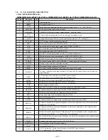
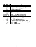
Pin No.
Pin Name
I/O
Description
39
HOLD
I
HOLD switch (S804) input terminal “L”: hold ON, “H”: hold OFF
40
EX BATT
I
External battery detection signal input terminal
41
XSPDOE
O
Control signal output to the spindle motor driver (IC402)
42
XHGON
O
Optical pick-up power ON/OFF control signal output terminal “L”: ON
43
XLAT
O
Serial data latch pulse signal output to the CXD3027R (IC601)
44
XSOE
O
Serial data output enable signal output terminal
45
DRVLT
O
Latch signal output to the spindle motor driver (IC402)
46
XPOWLT
O
Latch signal output to the power control (IC401)
47
XDOUTON
O
Digital output LED control signal output terminal “L”: ON
48
XAPC OFF
O
APC mute signal output terminal “L”: mute
49
XVRST
—
Not used (open)
50 to 64
SEG14 to SEG0
O
Segment drive signal output to the liquid crystal display on the switch unit
65 to 68
COM3 to COM1
O
Common drive signal output to the liquid crystal display on the switch unit
69 to 71
V3 to V1
O
Bias signal output to the liquid crystal display driver
72, 73
C1, C0
O
Capacitor connected terminal for the liquid crystal display driver voltage-up
74
STOP
O
VCD control stop signal output terminal Not used (Fixed at “L”)
75
TEST
I
Test terminal for IC (Fixed at “L”)
76
XHPSW
O
ON/OFF control signal output to the headphone amplifier (IC351)
77
XLIGHT
O
LCD back light control signal output to the liquid crystal display on the switch unit
78
RESET
I
System reset signal input from the power control (IC401) “L”: reset
For several hundreds msec. after the power supply rises, “L” is input, then it changes to “H”
79
XIN
I
System clock input terminal
80
XOUT
O
System clock input terminal Not used (open)


