8
D-NE509
SECTION 5
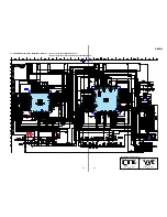
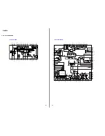
DIAGRAMS
5-1. IC PIN DESCRIPTIONS
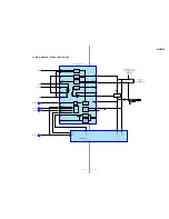
• IC601 CXD3048R (RF AMP, DIGITAL SIGNAL PROCESSOR, DIGITAL SERVO PROCESSOR, D-RAM CONTROLLER)
Pin No.
Pin Name
I/O
Pin Description
1
XRAS
O
Low address strobe signal output to the D-RAM
2
XWE
O
Data input enable signal output to the D-RAM
3 to 6
D1, D0, D3, D2
I/O
Two-way data bus with the D-RAM
7
DCLK
O
Not used (open)
8
DCKE
O
Not used (open)
9
XCAS
O
Column address strobe signal output to the D-RAM
10
WFCK/DQM
O
Not used (open)
11 to 13
A9 to A7
O
Address signal output to the D-RAM
14
DVSS
—
Ground
15 to 17
A6 to A4
O
Address signal output to the D-RAM
18
XRDE
I
D-RAM read enable signal input
19
VDD0
—
Power supply
20
CLOK
I
Serial data transfer clock signal input from TMP91CW28FG
21
SDTO
I
Serial data input from TMP91CW28FG
22
SENS
O
Serial data output to TMP91CW28FG
23
XLAT
I
Serial data latch pulse signal input from TMP91CW28FG
24
XSOE
I
Serial data output enable signal input from TMP91CW28FG
25
SYSM
I
Analog muting on/off control signal input from TMP91CW28FG “H”: muting on
26
WDCK
O
Not used (open)
27
SCOR
O
Subcode sync (S0+S1) detection signal output to TMP91CW28FG
28
XRST
I
Reset signal input from TMP91CW28FG “L”: reset
29
PWMI
I
Not used (fixed at “L”)
30
XQOK
I
Not used (fixed at “L”)
31
XWRE
I
Not used (fixed at “L”)
32
R8M
O
System clock output to TMP91CW28FG
33
VSS0
—
Ground
34
SQCK
I
SQSO readout clock signal input Not used (fixed at “H”)
35
SCLK
I
SENS serial data read clock signal input Not used (fixed at “H”)
36
SQSO
O
Not used (open)
37
XEMP
O
Not used (open)
38
XWIH
O
Not used (open)
39
SBSO
O
Not used (open)
40
EXCK
O
SQSO readout clock signal output Not used (pull down)
41
XTSL
I
Input terminal for the system clock frequency setting (pull down)
42
HVSS
—
Ground
43
HPL
O
Not used (open)
44
HPR
O
Not used (open)
45
HPVDD
—
Power supply
46
XVDD
—
Power supply
47
XTAI
I
System clock input (16.934 MHz)
48
XTAO
O
System clock output (16.934 MHz)
49
XVSS
—
Ground
50
AVDD1
—
Power supply
51
AOUT1
O
L-ch analog audio signal output
52
VREFL
O
L-ch reference voltage output
53, 54
AVSS1, AVSS2
—
Ground
55
VREFR
O
R-ch reference voltage output
56
AOUT2
O
R-ch analog audio signal output
57
AVDD2
—
Power supply
Summary of Contents for CD Walkman D-NE509
Page 29: ...29 D NE509 MEMO ...


