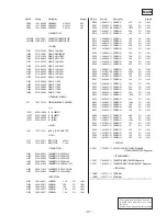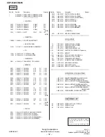
– 8 –
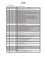
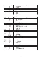
Pin No.
Pin name
I/O
Description.
1
VDD
–
+5V power supply
2
VSS
–
Ground
3
LMUT
O
Lch “L” detection flog (Not used)
4
RMUT
O
Rch “L” detection flog (Not used)
5
ACDT
O
Test output (Not used)
6
CKOUT
O
Master clock divider output (Not used)
7
SQCK
I
Clock input for SQSO read out
8
SQSO
O
Serial output for Sub-Q 80bit
9
SENS
O
SENS signal output to CPU
10
DATA
I
Serial data input, supplied from CPU
11
XLAT
I
Latch input, supplied from CPU
12
CLOK
I
Serial data transfer clock input, supplied from CPU
13
SEIN
I
SENS input from IC101
14
CNIN
I
Numbers of track jump counted signal input
15
DATO
O
Serial data output to IC101
16
XLTO
O
Serial data latch output to IC101
17
CLKO
O
Serial data transfer clock output to IC101
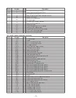
18
SPOA
I
Micro computer demodulation interface (Input A)
19
SPOB
I
Micro computer demodulation interface (Input B)
20
SPOC
I
Micro computer demodulation interface (Input C)
21
SPOD
I
Micro computer demodulation interface (Input D)
22
XLON
O
Micro computer demodulation interface (Output) (not used)
23
FOK
I
Focus OK input
24
VDD
–
+5V power supply
25
VSS
–
Ground
26
MON
O
Output to control ON/OFF of spindle motor (Not used)
27
MDP
O
Output to control spindle motor servo
28
MDS
O
Output to control spindle motor servo (Not used)
29
LOCK
O
GFS is sampled by 460Hz
30
PWMI
I
Input to control the outside spindle motor
31
TES0
I
Test pin (Connected to ground)
32
TES1
I
Test pin (Connected to ground)
33
VPCO2
O
Charge-pump output (Not used)
34
VPCO1
O
Charge-pump output (Not used)
35
VCKI
I
VCO2 oscillator input (Not used)
36
V16M
O
VCO2 oscillator output (Not used)
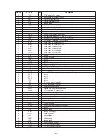
Pin No.
Pin name
I/O
Description.
41
F
I
F I-V and E I-V amplifier inverted input.
42
E
I
Connect these pins to photo diodes F and E.
43
EI
–
I-V amplifier E gain adjustment
(When not using automatic balance adjustment) (not used).
44
VEE
–
Negative power supply.
45
TEO
O
Tracking error amplifier output
E-F signal is output.
46
LPFI
I
Comparator input for balance adjustment
(Input from TEO through LPF).
47
TEI
I
Tracking error input.
48
ATSC
I
Window comparator input for ATSC detection.
49
TZC
I
Trackig zero-cross comparator input.
50
TDFCT
I
Capacitor connection pin for defect time constant.
51
VC
O
(VCC + VEE)/2 direct voltage output.
52
FZC
I
Focus zero-cross comparator input.
IC103 DIGITAL SIGNAL PROCESSOR (CXD2529Q)


