background image

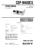
SERVICE MANUAL

Sony Corporation

Audio Group
Published by Sony Engineering Corporation

US Model

Canadian Model

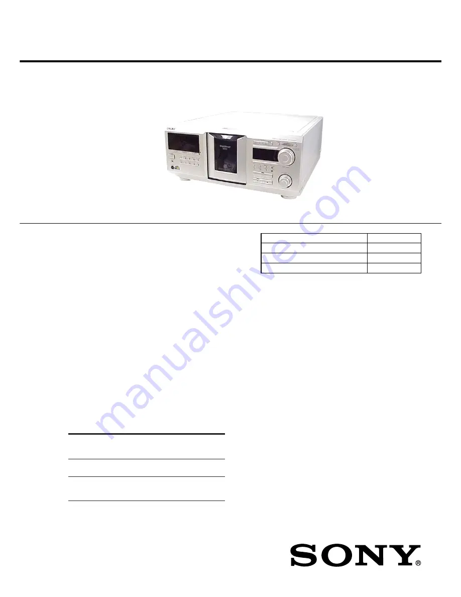
COMPACT DISC PLAYER

9-879-247-01

2004K1678-1
© 2004.11

Ver. 1.0  2004.11

SPECIFICATIONS

CDP-M400CS

Model Name Using Similar Mechanism

CDP-CX455

CD Mechanism Type

CDM62-K1BD46A

Base Unit Type

BU-K1BD46A

Optical Pick-up Type

KSM-213BFN

Compact disc player

Laser

Semiconductor laser (

λ

 = 780 nm)

Emission duration: continuous

Laser output

Max 44.6 

µ

W*

* This output is the value measured at

a distance of 200 mm from the
objective lens surface on the Optical
Pick-up block with 7 mm aperture.

Frequency response

20 Hz to 20 kHz 

±

0.5 dB

Signal-to-noise ratio

More than 108 dB

Dynamic range

More than 85 dB

Harmonic distortion

Less than 0.012%

Output

LINE OUT

DIGITAL OUT
(OPTICAL)

Jack
type

Phono
jacks

Optical
output
connector

Maximum
output
level

2 V
(at 50 kilohms)

–18 dBm

Load
impedance

Over 10 kilohms

Wave length: 660 nm

General

Power requirements

120 V AC, 60 Hz

Power consumption

16 W

Dimensions (approx.)

430 

×

 189 

×

 537 mm

(w/h/d)

(17 

×

 7 1/2 

×

 21 1/4 in.) incl. projecting

parts

Mass (approx.)

8.8 kg (19 lbs 7 oz.)

Supplied accessories

Design and specifications are subject to change without notice.

• Audio cord (1)
• Remote commander (remote) (1)
• Size AA (LR6) batteries (2)

Summary of Contents for CDP-M400CS Operating Instructions (CDPM400CS)

Page 1: ...bjective lens surface on the Optical Pick up block with 7 mm aperture Frequency response 20 Hz to 20 kHz 0 5 dB Signal to noise ratio More than 108 dB Dynamic range More than 85 dB Harmonic distortion Less than 0 012 Output LINE OUT DIGITAL OUT OPTICAL Jack type Phono jacks Optical output connector Maximum output level 2 V at 50 kilohms 18 dBm Load impedance Over 10 kilohms Wave length 660 nm Gene...

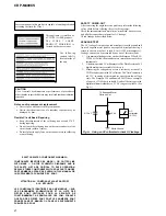
Page 2: ...M or battery operatedAC voltmeter The limit indication is 0 75 V so analog meters must have an accurate low voltage scale The Simpson 250 and Sanwa SH 63Trd are examples of a passive VOM that is suitable Nearly all battery operated digital multimeters that have a 2VAC range are suitable See Fig A Fig A Using an AC voltmeter to check AC leakage 1 5 kΩ 0 15 µF AC voltmeter 0 75 V To Exposed Metal Pa...

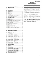
Page 3: ...DISPLAY Section 39 6 11 Printed Wiring Board JOG Section 40 6 12 Schematic Diagram JOG Section 41 6 13 Printed Wiring Board POWERSection 42 6 14 Schematic Diagram POWER Section 43 7 EXPLODED VIEWS 7 1 Case Section 51 7 2 Chassis Section 1 52 7 3 Chassis Section 2 53 7 4 Front Panel Section 54 7 5 Mechanism Section 1 CDM62 K1BD46A 55 7 6 Mechanism Section 2 CDM62 K1BD46A 56 7 7 Mechanism Section 3 ...

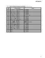
Page 4: ...EXT Display In this unit some special characters will not be displayed properly These will be displayed as a space or a character resembling it For details refer to Table 2 CD TEXT DISC Recorded Contents and Display Table 1 CD TEXT TEST DISC Text Data Contents TRACKS No 1 to 41 Normal Characters NOTE The contents of Track No 1 to 41 are the same as those of the current TEST DISC their titles are d...

Page 5: ...same 51 h i j k l m n o 68h to 6Fh T All the same 52 p q r s t u v w 70h to 77h T All the same 53 x y z I 78h to 7Fh T All the same 54 i A0h to A7h 8859 1 T All the same 55 C ª PR A8h to AFh T All the same 56 2 3 µ B0h to B7h T All the same 57 1 º B8h to BFh are displayed without 58 À Á Â Ã Ä Å Æ Ç C0h to C7h T All the same 59 È É Ê Ë Ì Í Î Ï C8h to CFh T All the same 60 D Ñ Ò Ó Ô Õ Ö D0h to D7h T...

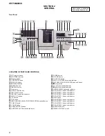
Page 6: ...LECT button and indicator wa FADER button ws X FADE button wd NO DELAY button wf MEGA CONTROL button and indicator wg l AMS L PUSH ENTER knob and button wh p stop button wj play button and indicator wk P pause button and indicator wl ARTIST MODE button and indicator e TOP ARTIST 4 button and indicator ea TOP ARTIST 3 button and indicator es TOP ARTIST 2 button and indicator ed TOP ARTIST 1 button ...

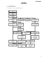
Page 7: ...ECTION Page 15 3 17 CD MECHANISM MAGNET ASSEMBLY Page 16 3 9 LED BOARD GUIDE DOOR Page 11 3 10 DOOR SW BOARD Page 12 3 14 T SENS BOARD HOLDER TABLE SENSOR 400 Page 14 3 18 LOADING SW BOARD LOCK SW BOARD Page 17 3 19 CDM ASSEMBLY Page 18 3 20 MOTOR ASSEMBLY TABLE M601 MOTOR ASSEMBLY LOADING M602 Page 18 3 21 BU HOLDER Page 19 3 22 BD BOARD OPTICAL PICK UP KSM 213BFN Page 19 3 15 D SENS OUT BOARD D ...

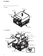
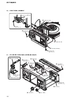
Page 8: ... screw 4 two screws case 3 screw 5 case qd two screws BVTP 3 8 qh bracket R 2 connector CN901 1 three connectors CN503 CN801 CN903 3 connector CNP902 6 connector CNP504 7 connector CNP1001 5 flat type wire CN502 17 core 4 two connectors CN505 CN506 8 three screws BVTP 3 8 9 four screws BVTP 3 8 qa MAIN board 0 flat type wire CN501 31 core qs two screws BVTP 3 8 qg bracket L qf ...

Page 9: ...S 3 4 TRANS BOARD 3 5 IR IN BOARD 5 screw BVTP 3 8 6 bracket PT 4 connector CN601 1 connector CN991 3 connector CN603 2 connector CN602 7 two screws PTTWH 3 6 8 TRANS board a a 1 two screws BVTP 3 8 2 IR IN board ...

Page 10: ...rews BVTP 3 8 7 remove the claw 8 remove the claw 9 front panel assembly 1 qs Remove two solderings 1 knob AMS 2 knob disc 3 four screws BVTP 2 6 8 4 bracket case assembly 5 eleven screws BVTP 2 6 8 7 eight screws BVTP 2 6 8 qa two screws BVTP 2 6 8 8 DISP board 9 flat type wire 17 core 0 knob timer 6 JOG board qf KEYBOARD board qd bracket keyboard ...

Page 11: ...D GUIDE DOOR 3 screw BVTP 3 16 4 guide door 5 table 400 assembly 6 washer Note during re assembling When re assembling align the positions as shown 1 two screws BVTP 3 8 2 cover PT 1 screw BVTP 3 8 6 window internal illumination 2 LED board 3 5 4 7 guide door ...

Page 12: ...in the illustration and rotate it fully in the direction of the arrow B 3 When the gear cam happens to go too deep return it to the original position in the direction of the arrow C 4 gear B 2 gear cam 6 DOOR SW board C B A lever pu joint two rotary switches slider pop up gear cam DOOR SW board The levers of the two rotary switches on the D SW board are shown in the illustration below Precaution d...

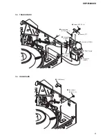
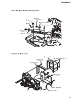
Page 13: ...RIVING ASSEMBLY 3 12 POP UP ASSEMBLY 1 connector CN602 2 three screws BVTP 3 8 3 cover table 4 door assembly 5 two screws BVTP 3 8 6 eight screws BVTP 3 8 7 base door driving assembly 1 screw PTPWH 3 6 2 step screw 3 pop up assembly ...

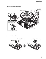
Page 14: ...NS BOARD HOLDER TABLE SENSOR 400 1 belt 3 D MOTOR board 5 door motor assembly 4 Remove two solderings 2 two screws BVTP 3 8 M603 1 four screws PTPWH 3 6 4 T SENS board 5 screw PTTWH 3 6 2 connector CN83 3 two connectors CN81 CN82 6 three claws 7 holder table sensor 400 ...

Page 15: ... PSW 3 8 6 D SENS OUT board 1 screw PTTWH 3 6 2 clamp 8 D SENS IN board 3 two step screws T1 4 bracket sensor 400 7 screw PTTWH 3 6 1 nine screws BVTP 3 8 2 cover CDM 3 three screws BVTP 3 8 4 bracket CDM 5 6 connector CN991 7 four screws BVTP 3 8 8 back panel section flat cable clamp ...

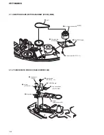
Page 16: ...ECHANISM MAGNET ASSEMBLY 2 three screws BVTP 3 8 1 three screws BVTP 3 8 3 bracket top 400 4 magnet assembly 5 washer 6 spring 7 CD mechanism 8 washer Note during re assembling When re assembling align the positions as shown ...

Page 17: ...y 400 in the direction of the arrow fully 2 screw BVTP3 8 5 tapping screw 4 belt 8 screw BVTP 3 8 0 screw BVTP 2 6 8 qa LOADING SW board 9 LOCK SW board 7 gear center 6 pulley 400 Note during re assembling When re assembling the LOADING SW board and LOCK SW boards align the leads position as shown LOADING SW board LOCK SW board Leads position ...

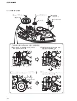
Page 18: ...NG M602 1 connector CN603 4 four screws BVTP 3 8 3 screw PSW 3 8 5 seven screws BVTP 3 8 6 CDM assembly 2 connector CN601 4 motor assembly loading M602 1 two belts 3 Remove two solderings 5 Remove two solderings 2 three screws PTPWH 2 6 8 6 motor assembly table M601 7 L T MOTOR board ...

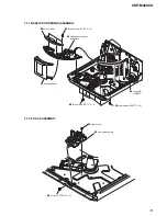
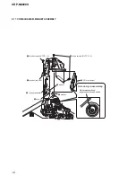
Page 19: ... 2 5 BU holder assy 3 tension spring F 1 4 tension spring F 2 2 screw B 2 5 8 two vibration proof rubbers 7 two vibration proof rubbers 1 wire flat type 31 core CN101 5 wire flat type 16 core CN102 6 BD board 9 optical pick up KSM 213BFN 4 Remove two solderings sled 3 Remove two solderings spindle ...

Page 20: ...he Ship mode the standby mode is automatically entered 3 Buttons Method To exit the mode press the 1 u button to enter the standby state When selecting the Ship mode the standby mode is automatically entered Contents Software version display BU test mode CDM test mode Normal aging mode Default mode Display Version BU Test CDM Test Aging Mode Ship Mode Power supply state ON ON ON ON ON Mode name DO...

Page 21: ...he state of the unit when errors occur Special Aging Mode Functions The aging mode is provided with the following convenient functions 1 Disc setting mode 5 discs are set before setting the aging mode This mode makes the setting of these discs more easy 2 Aging disc count function Functions which displays the number of aging discs carried out on the Fluorescent indicator tube in numbers Aging Proc...

Page 22: ... With no problem Error during table operation Code number 0X 1X Contents From chucking to TOC read From chucking to TOC read From TOC read to end of last track playback From TOC read to end of last track playback From end of last track playback to end of first track playback From end of last track playback to end of first track playback Code number 01 02 03 04 05 06 Contents With no problem With n...

Page 23: ...BUM CHARACTER dial select DoorPopup Aging and press the dial 4 Aging starts and door open close and up down operations of the pop up part are performed continuously 5 To end this mode press the 1 u button Procedure2 1 With the power ON while pressing the TOPARTIST 3 button and button press the 100 button 2 Aging starts and door open close and up down operations of the pop up part are performed con...

Page 24: ...r the following special buttons However these will not be displayed for the following special buttons x stop button FL segment check Refer to FL Tube Check Patterns P pause button FL grid check Refer to FL Tube Check Patterns The P LED also lights up simultaneously play button All FL segment and grid will light up LED also lights up simultaneously TIMER switch When the switch position is PLAY the ...

Page 25: ...ig 2 The following buttons have special functions in this mode TOP ARTIST 1 button Loading mechanism IN operation TOP ARTIST 5 button Loading mechanism OUT operation TOP ARTIST 2 button Pop up part UP operation TOP ARTIST 6 button Pop up part DOWN operation Fig 1 Fig 2 Table Sensor Adjustment 1 Enter the CDM Test mode and select Mech Adjust with the JOG dial and press the dial 2 Press the TOP ARTI...

Page 26: ...n A and B And confirm peak to peak level within 3 1 Vp p S curve waveform 6 Pressing the MENU NO button stops the output of the waveform S CURVE bdt S CURVE is displayed 7 To end this mode press the 1 button Note Try to measure several times to make sure than the ratio of A B or B A is more than 10 7 Take sweep time as long as possible and light up the brightness to obtain best waveform Adjustment...

Page 27: ...ble extent rotate the DISC ALBUM CHARACTER knob in the clockwise direction and the disc table starts to rotate in the same direction Repeat from step 4 6 Rotate RV501 of the MAIN board and adjust so that the H and L portions of the D S waveform become the same S tight screw PTTWH 3 6 D sens out board D SENS H H CH1 CH2 D SENS H H CH1 CH2 Should be at the center D SENS CH1 Adjust so that these widt...

Page 28: ...8 CDP M400CS BD BOARD Conductor Side Adjustment Location MAIN BOARD Component Side TP FE1 TP DVC TP RF AC IC 103 IC 101 TP1 TP AFADJ GND TP ADJ 1 3 RV501 DISC SENSOR ADJUSTMENT IC501 IC504 Conductor Side ...

Page 29: ...uction tolerances Circled numbers refer to waveforms Signal path J CD c digital out Abbreviation CND Canadian model Note The components identi fied by mark 0 or dot ted line with mark 0 are critical for safety Replace only with part number specified Note Les composants identifiés par une marque 0 sont cri tiques pour la sécurité Ne les remplacer que par une piéce portant le numéro spécifié For Pri...

Page 30: ...COR 95 SUBQ 15 TABLE SENSOR IC81 84 25 LDIN 26 DOORIN MOTOR DRIVE 6 7 8 2 IC961 LOADING M602 7 SENS SENS 6 OUT OPTICAL DIGITAL 3 1 LPF 2 1 AMP IC302 6 7 AMP IC302 Q324 MUTE Q322 MUTE Q323 MUTE Q321 325 326 328 329 MUTE CONT Q327 MUTE CONT 2ND CD IN 37 PO5 ANALOG OUT J903 IC501 1 2 SYSTEM CONTROL IC401 8 9 IC105 78 DOORSW 79 LDSW DOOR S612 DOWN UP POP UP S611 OPEN CLOSE LOADING S621 LOCK S622 4 3 M...

Page 31: ...6 80 KEY0 100 FLDATAI SOUT 14 16 BUSIN 14 BUSOUT 34 RESET Q950 CONTROL A1 II J901 J902 T911 D901 904 AC IN RELAY DRIVE Q901 IC930 T901 5V REG 2 3 RY991 5V REG 1 3 IC921 LINE FILTER L991 RECT D905 906 RECT IC931 5V REG RESET RST VIN 4 2 VOUT 5 MUTE 5V IC703 501 503 5V D931 934 RECT 7V REG 1 3 IC920 7V 5V M B M B D921 924 RECT 5V REG 1 3 FL702 DVDD 5V AU VCC AU VEE D911 RECT Q911 30V REG D913 Q941 2...

Page 32: ...N See page 29 for Circuit Boards Location Uses unleaded solder Semiconductor Location Ref No Location IC101 D 8 IC103 E 8 IC104 D 10 IC105 E 1 IC121 F 2 IC150 C 7 Q101 F 4 Page 34 13 13 13 13 1 2 A B C D E F 3 4 5 6 7 8 9 10 11 IC105 IC121 IC150 IC101 IC103 IC104 ...

Page 33: ...S CDP M400CS 6 3 SCHEMATIC DIAGRAM BD SECTION See page 29 for Waveforms See page 44 45 and 46 for IC Block Diagrams See page 47 for IC Pin Function Description No mark STOP IC B D IC B D IC B D 36 V C204 47p CH MSB710 ...

Page 34: ...E 17 2 16 5 IC402 IC910 IC921 IC920 IC401 IC501 IC504 IC302 IC901 IC931 IC930 Semiconductor Location Ref No Location D327 D 4 D329 D 3 D501 G 4 D502 H 7 D503 H 6 D551 G 8 D941 C 8 D942 C 8 IC302 F 3 IC401 E 4 IC402 E 3 IC501 G 6 IC504 G 7 IC901 F 2 IC910 B 4 IC920 C 3 IC921 B 3 IC930 B 4 IC931 B 5 Q321 D 5 Q322 E 3 Q323 E 2 Q324 D 2 Q325 D 3 Q326 E 5 Q327 D 4 Q328 D 3 Q329 D 3 Q421 D 5 Q422 E 2 Q4...

Page 35: ... Function Description No mark STOP 39 41 BS62LV256SC 70 T 4 7k 4 7k 10k DISP 37 39 36 43 uPD703030BYGF M13 3BA 37 36 41 MTZJ T 72 6 2B CN1101 PH4P R1004 G1002 C1002 G1001 TP1008 TP1007 TP1006 TP1005 TP1003 TP1004 TP1002 TP1001 R1005 R1006 J1001 R1001 C1009 CN1001 Q1001 C1001 C1007 10k 0 01 0 0 0 0 4P UN2214 0 1 0 1 ...

Page 36: ...36 36 CDP M400CS CDP M400CS 6 6 SCHEMATIC DIAGRAM MAIN SECTION 2 2 See page 45 for IC Block Diagrams No mark STOP 33 35 35 43 43 IC B D A A GP1FA550TZ ...

Page 37: ...s Location IC83 IC82 IC84 IC81 MAIN BOARD CN801 Page 34 Page 34 1 683 730 1 683 724 1 683 723 CN504 H 1 2 A B C D E F 3 4 5 6 8 SCHEMATIC DIAGRAM SENSOR SECTION Uses unleaded solder 4 9 4 1 4 9 4 9 4 9 4 9 4 9 0 4 9 0 1 1 1 1 1 1 1 1 No mark STOP Page 35 Page 35 B F CN504 CN801 1 2 1 2 DISC SENSOR ...

Page 38: ... BOARD MAIN BOARD CN503 Page 34 1 2 3 4 5 6 KEYBOARD 1 683 722 B Page 40 Page 34 63 S768 TIMER MODE E 13 13 13 13 IC701 IC702 IC703 1 2 A B C D E F G H 3 4 5 6 7 8 9 10 11 Semiconductor Location Ref No Location D701 E 5 D702 E 4 D703 E 3 D704 E 2 D705 E 2 D706 F 5 D707 F 4 D708 F 3 D709 F 2 D710 E 7 IC701 C 3 IC702 D 2 IC703 A 1 Q701 D 3 ...

Page 39: ...39 39 CDP M400CS CDP M400CS 6 10 SCHEMATIC DIAGRAM DISPLAY SECTION See page 44 for IC Block Diagrams No mark STOP 41 35 35 IC B D C703 0 1 M66310FP ...

Page 40: ...M400CS CDP M400CS 6 11 PRINTED WIRING BOARD JOG SECTION See page 29 for Circuit Boards Location Uses unleaded solder Page 34 Page 34 E Page 38 DISC EJECT 1 2 4 20 22 23 13 13 1 2 A B C D E F G H 3 4 5 6 7 8 IC704 ...

Page 41: ...41 41 CDP M400CS CDP M400CS 6 12 SCHEMATIC DIAGRAM JOG SECTION See page 44 for IC Block Diagrams No mark STOP IC B D 39 35 35 AFP PUSH ENTER ...

Page 42: ...683 726 1 683 725 1 683 728 BOARD 13 13 13 13 13 13 13 13 13 13 IC941 IC961 1 2 A B C D E 3 4 5 6 7 8 9 Semiconductor Location Ref No Location D901 B 2 D902 B 2 D903 B 2 D904 B 2 D905 B 2 D906 B 2 D907 B 1 D911 E 3 D912 E 4 D913 D 4 D921 D 3 D922 D 3 D923 E 3 D924 E 3 D931 D 3 D932 D 3 D933 D 3 D934 D 4 D935 C 3 D991 C 3 IC941 B 2 IC961 B 3 Q901 C 3 Q911 E 4 Q931 C 3 Q941 A 4 Q942 A 4 Q951 B 4 Q95...

Page 43: ...k STOP Page 36 CN902 2 2 J Page 36 2 2 CN901 I Page 35 1 2 CN903 H IC B D IC B D 2 2k 1 1 2 2k 2 2k MOTOR SWITCH 5V GND VCC AC IN RELAY F1 F2 V DISP AU VEE GND GND AU VCC GND M VCC 2 2k 2 2k 1k DOOR SW LOADING SW GND L MOTOR CONT L MOTOR CONT D MOTOR CONT D MOTOR CONT T MOTOR CONT T MOTOR CONT 30V REG 4 7k 10EDB40 TA2B5 10EDB40 TA2B5 10EDB40 TA2B5 10EDB40 TA2B5 10EDB40 TA2B5 10EDB40 TA2B5 10EDB40 ...

Page 44: ... VSSX CKO VDDP XI XO VRAR RO VDAR VDAL LO VRAL VSSL VSS STANDBY VDD LRCKIB 24 0 D R CK 23 0 D R CK 22 0 D R CK 21 0 D R CK 20 0 D R CK 19 0 D R CK 18 0 D R CK 17 0 D R CK 16 0 D R CK 15 0 D R CK 14 0 D R CK 13 4 5 6 7 8 9 10 11 12 0 D R CK 1 D R CK 1 D R CK 1 D R CK 1 D R CK 1 D R CK 1 D R CK 1 D R CK 1 D R CK 1 D R CK 1 D R CK 1 D R CK 1 D R CK D 1 R CK D 1 0 0 R CK D R CK D R CK 1 2 3 D 1 R CK D...

Page 45: ...29 28 DVC VCC DVC 27 26 25 24 RW ROM EQ 23 22 21 20 19 RFAC VCA VCC DVC RW ROM VC RW ROM DVC 3 A B C D B C A A A B C D B C D D 1 2 APC AMP 5 6 7 8 9 4 RFAC SUMMING AMP RW ROM APC OFF Hi Z RW ROM H L VOFST VC RW ROM 10 11 GM GM 18 17 16 B D A C 13 14 15 12 EQ IN LD PD GND A B C D AC SUM E F DVCC DVC RFAC SW DC OFST RFDCI RFDCO VC RFC VFC BST RFG VCC CEI CE TE BAL TE FEI FE TRANS Board IC941 IC961 L...

Page 46: ...MUTE DATA XLAT CLOK SENS SCLK ATSK WFCK XUGF XPCK GFS C2PO SCOR C4M WDCK DVSS0 COUT MIRR AVDD0 IGEN AVSS0 ADIO RFDC CE TE AVSS1 RFAC ASYI ASYO BIAS AVDD1 PCO FILI FILO CLTV V16M VCTL VPCO 59 58 57 56 55 54 53 52 51 50 49 48 47 46 45 44 43 42 41 1 2 3 4 5 6 7 8 9 10 11 12 13 14 15 16 17 18 19 20 21 22 23 24 25 26 27 28 29 30 31 32 33 34 35 36 37 38 39 40 80 79 78 77 76 75 74 73 72 71 70 69 68 67 66...

Page 47: ...DAC Lch 22 VRAL Reference voltage terminal for DAC Lch 23 LO O DAC Lch signal output 24 VDAL Power supply 2 5V for DAC Lch 25 VDAR Power supply 2 5V for DAC Rch 26 RO O DAC Rch signal output 27 VRAR Reference voltage terminal for DAC Rch 28 VSSR Ground for DAC Rch 29 TESTP I Terminal for test H test mode L normal fixed at L 30 DOUT O SPDIF signal output open 31 to 34 PO0 to PO3 O General purpose o...

Page 48: ...I Flag signal input 2 SUBQ interface block sync input fixed at L 56 VSSP Ground for VCO circuit 57 PDO O PLL phase error detection signal output 58 VCOI I VCO control voltage input 59 VDDP Power supply 2 5V for VCO circuit 60 CKO O External clock output 61 VDDX Power supply 2 5V for oscillation circuit 62 XI I Resonator terminal input 63 XO O Resonator terminal output 64 VSSX Ground for oscillatio...

Page 49: ...put to the DSP 21 IC VPP Connected to ground 22 TBLR O Table motor control signal output clockewise 23 TBLL O Table motor control signal output counterclockewise 24 LDOUT O Loading motor control signal output out 25 LODIN O Loading motor control signal output in 26 DOORIN O Door motor control signal output close 27 DOOROUT O Door motor control signal output open 28 ICSW O Power supply to the perip...

Page 50: ...D 80 KEY0 I Key data signal input A D 81 DJOG2 I Jog signal input 82 TJOG2 I AMS jog signal input 83 TJOG1 I AMS jog signal input 84 DJOG1 I Jog signal input 85 KBDI I Keyboard data input 86 DSENS I Disc sensor signal input 87 TSENS1 I Table sensor signal input 88 TSENS3 I Table sensor signal input 89 KBDO O Keyboard data output 90 POWER I POWER key signal input 91 TSENS2 I Table sensor signal inp...

Page 51: ...e items Abbreviation CND Canadian model Ref No Part No Description Remark 1 4 985 553 11 CUSHION 2 A 1082 286 A MAIN BOARD COMPLETE 3 3 383 699 01 CLAMP EDGE 4 3 363 099 11 SCREW CASE 3 TP2 7 1 CASE SECTION Ref No Part No Description Remark The components identified by mark 0 or dotted line with mark 0 are critical for safety Replace only with part number specified Les composants identifiés par un...

Page 52: ... 63 4 226 876 21 COVER CDM 64 1 683 730 13 LED BOARD 0CNP901 1 783 820 21 CORD POWER 0T901 1 437 709 11 TRANSFORMER POWER 0T911 1 435 327 11 TRANSFORMER POWER 1 7 685 646 79 SCREW BVTP 3X8 TYPE2 IT 3 4 7 685 903 11 SCREW PTPWH 3X6 TYPE2 59 60 63 CNP901 1 1 1 1 1 1 not supplied not supplied not supplied CHASSIS SECTION 2 not supplied 61 62 T911 T901 MECHANISM SECTION 1 CDM62 K1BD46A 54 1 56 55 1 52...

Page 53: ...ER ROLLER 109 4 965 822 01 FOOT 110 X 2022 049 1 FOOT ASSY 111 4 216 088 02 GUIDE DISC 112 1 676 828 11 T SENS BOARD 113 1 683 724 13 D SENS OUT BOARD 114 1 683 723 13 D SENS IN BOARD 1 7 685 646 79 SCREW BVTP 3X8 TYPE2 IT 3 4 7 685 903 11 SCREW PTPWH 3X6 TYPE2 5 7 685 645 79 SCREW BVTP 3X6 TYPE2 N S 7 7 682 948 01 SCREW PSW 3X8 not supplied 1 5 5 5 1 1 1 7 1 1 109 110 106 108 107 not supplied 104...

Page 54: ...7 216 71 KNOB TIMER 159 A 4727 719 A DISP BOARD COMPLETE 160 3 087 053 01 BVTP2 6 3CR 161 A 4727 721 A JOG BOARD COMPLETE 162 4 982 811 21 HOLDER FL 163 4 929 709 31 GUIDE FL TUBE 164 1 683 722 13 KEYBOARD BOARD FL701 1 518 802 11 INDICATOR TUBE FLUORESCENT FL702 1 518 803 11 INDICATOR TUBE FLUORESCENT 160 159 158 162 157 160 160 164 163 160 156 157 160 160 160 161 152 153 155 151 154 not supplied...

Page 55: ...10 4 228 352 01 LEVER POP UP 400 211 4 216 104 01 SPRING POP UP TENSION 212 4 219 326 01 BELT DIA 42X1 2 213 3 701 441 21 WASHER 214 4 226 828 02 GEAR CAM 215 4 226 829 01 GEAR PULLEY 216 4 226 831 01 GEAR B 217 4 226 830 01 GEAR A 218 3 087 053 01 BVTP2 6 3CR 219 1 683 728 13 DOOR SW BOARD 220 1 683 729 13 D MOTOR BOARD M603 1 541 632 12 MOTOR DC DOOR 1 7 685 646 79 SCREW BVTP 3X8 TYPE2 IT 3 6 7 ...

Page 56: ... 216 081 01 SPRING MG TORSION 252 3 701 441 21 WASHER 253 3 701 446 21 WASHER 8 254 4 216 082 11 HOLDER MAGNET TORSION 255 A 4672 768 A MAGNET ASSY Ref No Part No Description Remark Ref No Part No Description Remark 256 X 4950 901 5 HOLDER ASSY BU 257 4 216 086 01 SPRING F 2 TENSION 258 4 216 085 01 SPRING F 1 TENSION 259 4 957 577 01 SCREW PTP WH 2 6X8 DIA 10 260 4 992 054 11 RUBBER VIBRATION PRO...

Page 57: ...CLAMP COMPRESSION 303 3 701 441 21 WASHER 304 X 4952 501 1 HOLDER DISC L400 ASSY 305 X 4952 502 1 HOLDER DISC R400 ASSY 306 4 225 868 01 SHAFT CLAMP 400 307 3 325 697 21 WASHER 308 4 216 076 11 HOLDER R 309 4 216 077 01 SPRING HOLDER FR TORSION 310 4 225 871 03 HOLDER F400 311 X 4950 900 1 BRACKET LEVER ASSY 312 4 216 080 01 SPRING LIMITTER TORSION 313 4 216 079 02 LIMITTER LEVER 314 4 216 078 01 ...

Page 58: ... PTPWH M2 6X8 354 A 4672 676 B CAM ASSY 355 4 225 876 01 BELT 400 356 4 225 870 01 PULLEY 400 357 4 216 057 01 GEAR CENTER 2 358 4 216 058 01 GEAR CENTER 359 3 087 053 01 BVTP2 6 3CR 360 4 225 869 01 GEAR TABLE 400 361 1 683 727 13 L T MOTOR BOARD 362 1 683 725 13 LOCK SW BOARD 363 1 683 726 13 LOADING SW BOARD M601 A 4672 895 A MOTOR 400 ASSY TABLE M602 A 4672 895 A MOTOR 400 ASSY LOADING 1 7 685...

Page 59: ...A 4727 735 A BD BOARD COMPLETE 0403 A 3328 818 A OPTICAL PICK UP KSM 213BFN C2N1 The components identified by mark 0 or dotted line with mark 0 are critical for safety Replace only with part number specified Les composants identifiés par une marque 0 sont critiques pour la sécurité Ne les remplacer que par une pièce portant le numéro spécifié ...

Page 60: ...7 1 164 360 11 CERAMIC CHIP 0 1uF 16V C208 1 164 360 11 CERAMIC CHIP 0 1uF 16V C209 1 162 927 11 CERAMIC CHIP 100PF 5 50V C211 1 107 826 11 CERAMIC CHIP 0 1uF 10 16V C212 1 162 966 11 CERAMIC CHIP 0 0022uF 10 50V C213 1 162 967 11 CERAMIC CHIP 0 0033uF 10 50V C215 1 117 863 11 CERAMIC CHIP 0 47uF 10 6 3V C216 1 107 726 91 CERAMIC CHIP 0 01uF 10 16V C222 1 164 360 11 CERAMIC CHIP 0 1uF 16V C223 1 1...

Page 61: ...25 11 METAL CHIP 2 2K 5 1 10W R205 1 216 821 11 METAL CHIP 1K 5 1 10W R206 1 216 825 11 METAL CHIP 2 2K 5 1 10W R207 1 216 857 11 METAL CHIP 1M 5 1 10W R213 1 216 864 11 SHORT CHIP 0 R214 1 216 864 11 SHORT CHIP 0 R215 1 216 864 11 SHORT CHIP 0 R216 1 216 857 11 METAL CHIP 1M 5 1 10W R218 1 216 821 11 METAL CHIP 1K 5 1 10W R219 1 216 821 11 METAL CHIP 1K 5 1 10W R220 1 216 821 11 METAL CHIP 1K 5 1...

Page 62: ...R785 1 247 807 31 CARBON 100 5 1 4W R786 1 247 843 11 CARBON 3 3K 5 1 4W R787 1 247 879 91 CARBON 100K 5 1 4W R788 1 247 807 31 CARBON 100 5 1 4W R789 1 247 807 31 CARBON 100 5 1 4W R790 1 249 409 11 CARBON 220 5 1 4W R791 1 249 409 11 CARBON 220 5 1 4W R792 1 249 409 11 CARBON 220 5 1 4W R793 1 249 413 11 CARBON 470 5 1 4W SWITCH S741 1 771 349 21 SWITCH KEYBOARD TOP ARTIST 1 S742 1 771 349 21 SW...

Page 63: ... 5 1 4W R731 1 249 429 11 CARBON 10K 5 1 4W R741 1 249 429 11 CARBON 10K 5 1 4W R751 1 249 429 11 CARBON 10K 5 1 4W R771 1 247 807 31 CARBON 100 5 1 4W R772 1 249 407 11 CARBON 150 5 1 4W R773 1 249 407 11 CARBON 150 5 1 4W R774 1 247 807 31 CARBON 100 5 1 4W R775 1 247 807 31 CARBON 100 5 1 4W R794 1 247 807 31 CARBON 100 5 1 4W ROTARY ENCODER RE701 1 475 543 11 ENCODER ROTARY DISC ALBUM CHARACTE...

Page 64: ...MIC 0 1uF 50V C504 1 164 159 11 CERAMIC 0 1uF 50V C505 1 164 159 11 CERAMIC 0 1uF 50V C508 1 161 494 00 CERAMIC 0 022uF 25V C509 1 161 494 00 CERAMIC 0 022uF 25V C510 1 161 494 00 CERAMIC 0 022uF 25V C511 1 161 494 00 CERAMIC 0 022uF 25V C512 1 161 494 00 CERAMIC 0 022uF 25V C513 1 164 159 11 CERAMIC 0 1uF 50V C514 1 164 159 11 CERAMIC 0 1uF 50V C515 1 161 494 00 CERAMIC 0 022uF 25V C516 1 164 159...

Page 65: ... TRANSISTOR 2SC3622A LK Q425 8 729 900 65 TRANSISTOR DTA144ES Q426 8 729 029 46 TRANSISTOR DTA143ESA Q501 8 729 900 89 TRANSISTOR DTC144ES Q502 8 729 029 46 TRANSISTOR DTA143ESA Q551 8 729 030 08 TRANSISTOR DTC144VSA Q552 8 729 900 65 TRANSISTOR DTA144ES Q562 8 729 900 65 TRANSISTOR DTA144ES Q570 8 729 116 02 TRANSISTOR BA1A4M TP Q571 8 729 116 02 TRANSISTOR BA1A4M TP Q572 8 729 116 02 TRANSISTOR ...

Page 66: ...5 1 4W R545 1 249 429 11 CARBON 10K 5 1 4W R546 1 247 807 31 CARBON 100 5 1 4W R550 1 249 429 11 CARBON 10K 5 1 4W R551 1 249 429 11 CARBON 10K 5 1 4W R552 1 247 807 31 CARBON 100 5 1 4W R553 1 247 807 31 CARBON 100 5 1 4W R554 1 247 807 31 CARBON 100 5 1 4W R570 1 247 847 91 CARBON 4 7K 5 1 4W R571 1 247 847 91 CARBON 4 7K 5 1 4W R591 1 247 847 91 CARBON 4 7K 5 1 4W R931 1 247 887 00 CARBON 220K ...

Page 67: ...ISTOR DTC144ES RESISTOR R901 1 247 831 91 CARBON 1K 5 1 4W R902 1 249 429 11 CARBON 10K 5 1 4W R903 1 249 421 11 CARBON 2 2K 5 1 4W R904 1 249 429 11 CARBON 10K 5 1 4W R911 1 247 847 91 CARBON 4 7K 5 1 4W R912 1 249 421 11 CARBON 2 2K 5 1 4W R913 1 247 847 91 CARBON 4 7K 5 1 4W R914 1 247 807 31 CARBON 100 5 1 4W R931 1 249 421 11 CARBON 2 2K 5 1 4W R932 1 249 421 11 CARBON 2 2K 5 1 4W R940 1 247 ...

Page 68: ...37 709 11 TRANSFORMER POWER 0T911 1 435 327 11 TRANSFORMER POWER ACCESSORIES 1 477 214 11 COMMANDER STANDARD RM DX455 1 790 735 12 CORD CONNECTION AUDIO 2 546 621 11 MANUAL INSTRUCTION ENGLISH 2 546 621 21 MANUAL INSTRUCTION FRENCH 4 228 696 01 COVER BATTERY FOR RM DX455 The components identified by mark 0 or dotted line with mark 0 are critical for safety Replace only with part number specified L...

Page 69: ...69 CDP M400CS MEMO ...
Page 70: ...STORY Clicking the version allows you to jump to the revised page Also clicking the version at the upper right on the revised page allows you to jump to the next revised page Ver Date Description of Revision 1 0 2004 11 New ...

Reviews: