58
CDX-5V661/5V661A/5V661D/5V661S
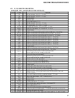
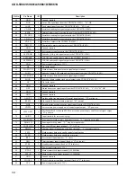
Pin No.
Pin Name
I/O
Description
44
GND
—
Ground terminal
45
FOK
I
Focus OK signal input from the CXD3027R (IC601) “H”: OK
46
LOCK
I
Lock signal input from the CXD3027R (IC601) “H”: Lock
47
CD SCK
O
Serial data reading for signal output to the CXD3027R (IC601)
48
SENS
I
Internal status signal (sens signal) input from the CXD3027R (IC601)
49
CD CKO
O
Serial data writing for signal output to the CXD3027R (IC601)
50
CD LAT
O
Serial data latch pulse signal output to the CXD3027R (IC601)
51
CD SO
O
Serial data output to the CXD3027R (IC601)
52
CDMUTE
O
Digital audio mute signal output to the CXD3027R (IC601)
53
GND
—
Ground terminal
54
CD RST
O
System reset signal output to the CXD3027R (IC601)
55
ESPXQOK
O
Subcode Q OK pulse signal output to the CXD3027R (IC601)
56
ESPXRDE
O
D-RAM read enable signal output to the CXD3027R (IC601)
57
ESPXWRE
O
D-RAM write enable signal output to the CXD3027R (IC601)
58
VDD
—
Power supply terminal (+3.3V)
59
NC
O
Not used (open)
60
FLASH TX
O
Flash memory data transfer write signal output terminal
61
SQSO
I
Subcode Q data, PCM peak and level data input from the CXD3027R (IC601)
62
FLASH RX
I
Flash memory data transfer write signal input terminal
63
SQCK
O
Subcode Q data reading clock signal output to the CXD3027R (IC601)
64
NC
O
Not used (open)
65
GND
—
Ground terminal
66
GFS
I
Guard frame sync signal input from the CXD3027R (IC601) “L”: NG, “H”: OK
67
GND
—
Ground terminal
68
GND
—
Ground terminal
69
AMUTE
O
Analog audio line muting on/off control signal output “H”: muting on
70
RF SW
O
Advanced ESP/normal setting terminal “H”: normal
71
MDS
I
Spindle motor positive/negative signal input from the CXD3027R (IC601)
72
CD PW
O
Servo section power supply on/off control signal output “H”: power on
73
MECA PW
O
Mechanism deck section and PANA bus section power supply on/off control signal output
“H”: power on
74
AGING
I
Input terminal for test mode (aging)
75
FLASH SW
I
Sens input for flash memory data transfer write “L”: transfer write mode
76
DIAG SW
I
Sens input for diag mode “L”: diag data input mode
77
CONTVOL
I
Acc sens (CD on) input terminal “L”: ACC on
78
DIMIN
I
Dimmer signal (illumination sens) input terminal “L”: dimmer signal in
79
FL W
O
Flash memery data write enable control signal output
80
FL EN
I
Flash memory data write enable input terminal
81
RST
I
System reset input terminal “L”: reset
82
NMI
I
Interrupt signal input terminal (fixed at “H” in this set)
83
STBY
I
Standby input terminal (fixed at “H” in this set)
84
VCC
—
Power supply terminal (+3.3V)
85
XTAL
I
Main system clock input terminal (12.288MHz)
86
EXTAL
O
Main system clock output terminal (12.288MHz)
87
GND
—
Ground terminal
88
MODEL
I
Model selection signal input terminal (fixed at “L” in this set)
89
VCC
—
Power supply terminal (+3.3V)


