– 23 –
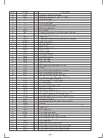
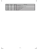
4-1. IC PIN DESCRIPTIONS
• IC5 CXP84640-050Q (CD SYSTEM CONTROL)
Pin No.
Pin Name
I/O
Pin Description
1 – 5
NCO
—
Not used in this set.
6
FP OPEN
I
Front panel open detection input
7
FP CLOSE
O
Front panel close control output
8
LINKOFF
I
Bus interface link input (Not used in this set.)
9
DRV OE
O
Focus/tracking coil/sled motor control output
10
D SW
I
Down switch input (SW4)
11 – 13
NCO
—
Not used in this set.
14
LM EJ
O
Loading motor control output
15
LM LOD
O
Loading motor control output
16
EMPH O
O
De-emphasis ON/OFF control output
17
CDMON
O
CD mechanism deck power control output
18
CD ON
O
CD power control output
19
A MUT
O
System attenuate control output
20
LD ON
O
Laser power ON/OFF control output
21
CD RST
O
CD system reset output
22 – 24
—
—
Not used in this set.
25
PH3
I
Not used in this set.
26
TSTIN0
I
Not used in this set.
27
TSTIN1
I
Not used in this set.
28
TST CLV
I
Not used in this set.
29
NCO
—
Not used in this set.
30
RESET
I
System reset input (“L” = Reset)
31
X IN
I
X’tal oscillator input of system clock. (10 MHz)
32
X OUT
O
X’tal oscillator output of system clock. (10 MHz)
33
GND
—
Analog GND
34
XT OUT
O
Not used in this set.
35
XT IN
I
Not used in this set.
36
AVSS
—
A/D converter GND
37
AVREF
I
A/D converter reference voltage input
38
TEP L
I
Not used in this set.
39
TEP H
I
Not used in this set.
40
NCO
—
Not used in this set.
41
PH2
I
Not used in this set.
42
SCLK
O
CD-TEXT data read clock output
43
ESPXQOK
O
XQOK signal output to DRAM controller.
44
ESPSDT
I
Serial data input from DRAM controller.
45
GRSRST
O
Reset signal output to DRAM controller.
46
GRSCOR
I
Sub-cord sync input from DRAM controller.
47
CD XLAT
O
CD signal process serial latch output
48
TX CLK
O
EEPROM serial clock output
49
TX DATA
O
EEPROM serial data output
50
UNISO
O
Not used in this set.
51
BUS CLK
I/O
Bus system serial clock input/output
52
BUS SI
I
Bus system serial interface input
53
BUS SO
O
Bus system serial interface output
54
F OK
I
Focus OK signal input
55
GFS
I
GFS signal detection input
56
SCOR
O
Sub-cord sync output
57
SENS
I
SENS signal input
58
—
I
Fixed at “H” in this set.
59
CD CKO
O
CD signal process serial clock output
SECTION 4
DIAGRAMS
Summary of Contents for CDX-C7850R
Page 3: ... 3 SECTION 1 GENERAL This section is extracted from instruction manual ...
Page 4: ... 4 ...
Page 5: ... 5 ...
Page 6: ... 6 ...
Page 7: ... 7 ...
Page 8: ... 8 ...
Page 9: ... 9 ...
Page 10: ... 10 ...
Page 11: ... 11 ...
Page 12: ... 12 ...
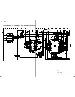
Page 39: ... 47 48 CDX C7850R Page 51 ...
Page 41: ...CDX C7850R 51 52 Page 65 Page 66 Page 47 ...
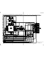
Page 49: ... 67 4 18 SCHEMATIC DIAGRAM RELAY SECTION Page 63 Page 60 Page 60 CDX C7850R ...

