25
25
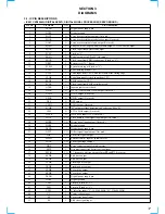
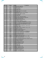
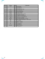
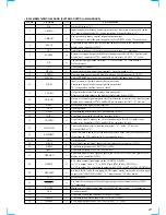
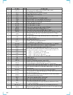
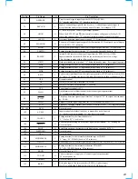
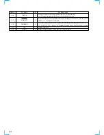
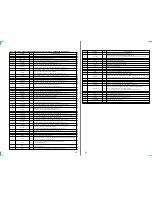
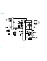
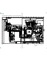
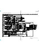
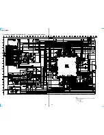
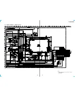
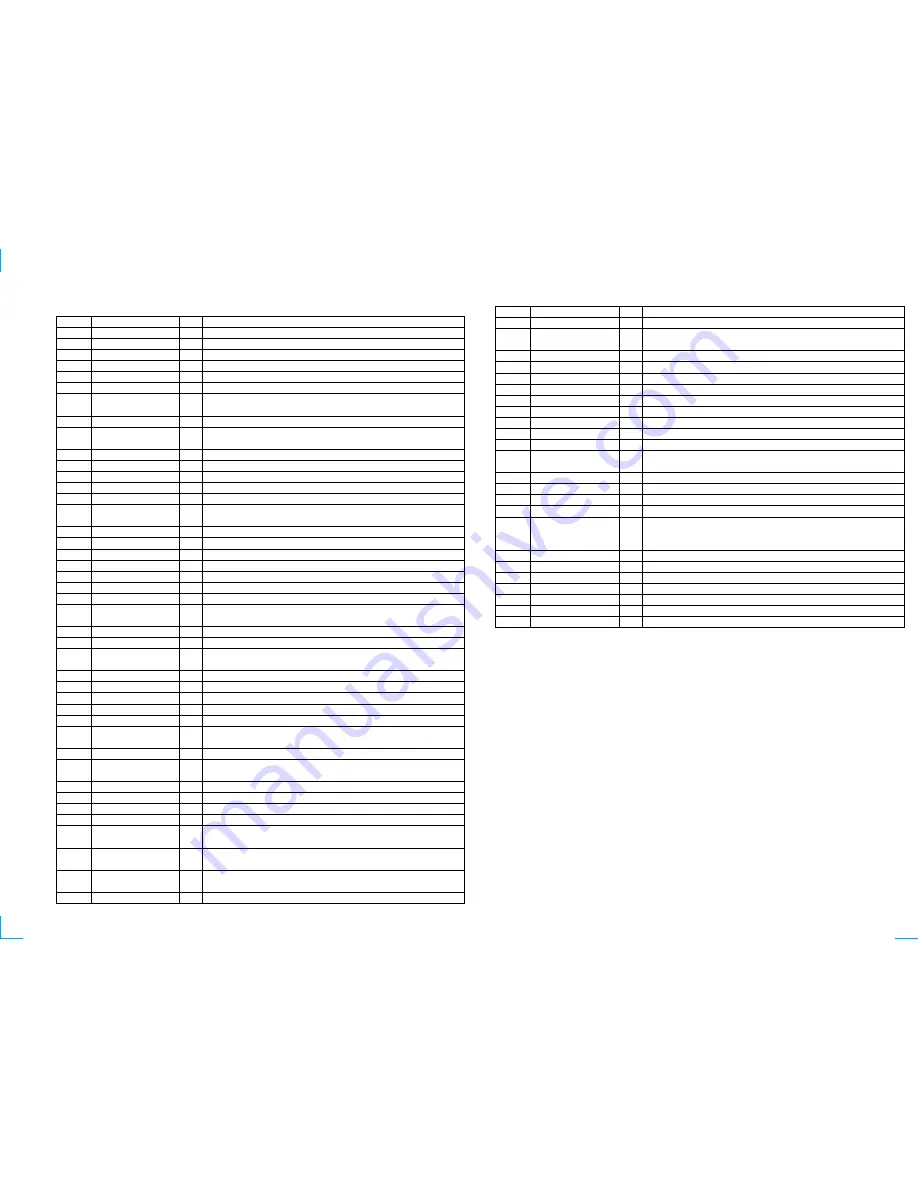
• IC805 CXD2726Q-4 (DIGITAL SIGNAL PROCESSOR, DIGITAL FILTER, D/A CONVERTER) (DSO BOARD)
Pin No.
Pin Name
I/O
Pin Description
1
DGND
—
Ground terminal (digital system)
2 – 15
T.P
I
Input terminal for the test (fixed at “L”)
16 – 21
TST0 – TST5
I
Input terminal for the test (fixed at “L”)
22 – 24
JPE1 – JPE3
I
External condition jump terminal “H”: condition jump (fixed at “L”)
25
DVDD
—
Power supply terminal (+3.3 V) (digital system)
26
DA1GND
—
Ground terminal (for D/A converter 1) (analog system)
27
DA1LO
O
D/A converter 1 (L-ch side) output terminal
Analog signal output for front side (L-ch side) output in this set
28
DA1VDD
—
Power supply terminal (+3.3 V) (for D/A converter 1) (analog system)
29
DA1RO
O
D/A converter 1 (R-ch side) output terminal
Analog signal output for rear side (L-ch side) output in this set
30
DA1VDD
—
Power supply terminal (+3.3 V) (for D/A converter 1) (analog system)
31
DA1GND
—
Ground terminal (for D/A converter 1) (analog system)
32
ADLVDD
—
Power supply terminal (+3.3 V) (for L-ch side A/D converter) (analog system)
33
ADLGND
—
Ground terminal (for L-ch side A/D converter) (analog system)
34
ADLREF
O
Connected to the bus control for A/D converter (for L-ch side)
35
ADLIN
I
A/D converter (L-ch side) analog input terminal
Tuner and bus audio input signal (L-ch side) in this set
36
DA2GND
—
Ground terminal (for D/A converter 2) (analog system)
37
DA2VDD
—
Power supply terminal (+3.3 V) (for D/A converter 2) (analog system)
38
DA2LO
O
D/A converter 2 (L-ch side) output terminal (Not used.)
39
MCKVDD
—
Power supply terminal (+3.3 V) (for master clock) (analog system)
40
MCKO
O
System clock output terminal (16.9344 MHz)
41
MCKI
I
System clock input terminal (16.9344 MHz)
42
MCKGND
—
Ground terminal (for master clock) (analog system)
43
DA2RO
O
D/A converter 2 (R-ch side) output terminal
Analog signal output for sub woofer output in this set
44
DA2VDD
—
Power supply terminal (+3.3 V) (for D/A converter 2) (analog system)
45
DA2GND
—
Ground terminal (for D/A converter 2) (analog system)
46
ADRIN
I
A/D converter (R-ch side) analog input terminal
Tuner and bus audio input signal (R-ch side) in this set
47
ADRREF
O
Connected to the bus control for A/D converter (for R-ch side)
48
ADRGND
—
Ground terminal (for R-ch side A/D converter) (analog system)
49
ADRVDD
—
Power supply terminal (+3.3 V) (for R-ch side A/D converter) (analog system)
50
DA3GND
—
Ground terminal (for D/A converter 3) (analog system)
51
DA3VDD
—
Power supply terminal (+3.3 V) (for D/A converter 3) (analog system)
52
DA3LO
O
D/A converter 3 (L-ch side) output terminal
Analog signal output for rear side (R-ch side) output in this set
53
DA3GND
—
Power supply terminal (+3.3 V) (for D/A converter 3) (analog system)
54
DA3RO
O
D/A converter 3 (R-ch side) output terminal
Analog signal output for front side (R-ch side) output in this set
55
DA3GND
—
Ground terminal (for D/A converter 3) (analog system)
56
DGND
—
Ground terminal (digital system)
57
SYSRST
I
System reset signal input from the master controller (IC502) “L”: reset
58
BFOT
O
Master clock signal output terminal
59
SCK
I
Serial data transfer clock signal input from the master controller (IC502) and liquid
crystal display drive controller (IC701)
60
REDY
O
Transfer enable signal output to the master controller (IC502)
“L”: transfer prohibition
61
TRDT
O
Serial data output to the master controller (IC502) and liquid crystal display drive
controller (IC701)
62
XLAT
I
Serial data latch pulse input from the master controller (IC502)
Pin No.
Pin Name
I/O
Pin Description
63
RVDT
I
Serial data input from the master controller (IC502)
64
24/23BIT
I
Serial data 24/32 bit slot selection signal input terminal
“L”: 24 bit slot, “H”: 32 bit slot (validity at slave mode) (fixed at “L” in this set)
65
DVDD
—
Power supply terminal (+3.3 V) (digital system)
66
DVSS
—
Ground terminal (digital system)
67 – 69
SO1 – SO3
O
Serial data output terminal (Not used.)
70
SOUT
O
Serial data output terminal (Not used.)
71
SI1
I
Serial data input terminal
72, 73
SI2, SI3
I
Serial data input terminal Not used (fixed at “L”)
74
SIN
I
Serial data input terminal Not used (fixed at “L”)
75
BCK
I
Bit clock signal (2.8224 MHz) input terminal
76
LRCK
I
L/R sampling clock signal (44.1 kHz) input terminal
77
MST/SLV
I
Bit clock (BCK) and L/R sampling clock (LRCK) signal master/slave mode selection
signal input from the master controller (IC502) “L”: master mode, “H”: slave mode
78
DVDD
—
Power supply terminal (+3.3 V) (digital system)
79
PLLGND
—
Ground terminal (PLL system)
80
PLLENA
I
PLL enable signal input terminal Normally: fixed at “L”
81
22 MHz
O
PLL clock signal output terminal (22.5792 MHz) (Not used.)
82
PLLCNT
I
PLL clock output control signal input from the master controller (IC502)
At “L” is input: fixed at “L” is PLCLK (pin
ia
)
At “H” is input: PLL clock signal output from the PLCLK (pin
ia
)
83
PLLVDD
—
Power supply terminal (+3.3 V) (PLL system)
84
DGND
—
Ground terminal (digital system)
85 – 94
T.P
I
Input terminal for the test Normally: fixed at “L”
95
DVDD
—
Power supply terminal (+3.3 V) (digital system)
96
DRAMGND
—
Ground terminal (for D-RAM)
97 – 99
T.P
I
Input terminal for the test Normally: fixed at “L”
100
DRAMVDD
—
Power supply terminal (+3.3 V) (for D-RAM)

