


CDX-GT572
CDX-GT572
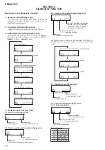
19
19
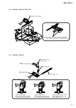
1
A
B
C
D
E
F
G
H
I
2
3
4
5
6
7
8
9
10
11
12
13
12
C414
C413
C432
C452
C442 C422
R432
R452
R442 R422
Q440
Q420
C423
C443
Q460
Q470
R35
7
R481
R480
R482
C482
C483
C484
R2
R3
R4
R5
D2
C7
R10
C3
C9
C8
C323
C324
C320
C313
C315
C902
C901
C704
D606
D605
D602
Q605
R60
3
R604
R611
D603
D604
Q601
R608
R610
R606
R607
R706
D702
D701
R708
R707
Q702
C415
C402
R351
FB408
FB407
FB406
FB405
FB404
FB401
FB402
FB403
C412
R402
R401
C419
C418
C601
R543
IC602
R522
R531
R532
R534
R601
R602
R536
C516
C515
C506
R370 R546
R529
R530 R528
R547
D502
R541
R550
R526
R525
C50
7
C508
R540
C509
R516
R548
R549
R545
C318
R301
R509
R510
R519
R520
D501
C50
2
C325
D491
R491
Q501
L500
L4
R553
C14
R500
JC501
JC503
JC491
JC490
JC302
JC300
JC301
JC3
JC600
JC350
C519
R527
R471
R539
C513
C410
C63
C64
C52
3
C110
D10
3
C104
D101
R494
R555
R556
R537
JC304
R411
C411
R461
R559
D114
D115
R418
Q589
Q590
R361
JC305
Q430
R416
Q492
Q491
D511
D494
D49
3
D400
R56
3
C4
C472
R433
R513
JC524
C116
C117
R501
R503
C331
C330
R455
R474
R355
R356
R419
R417
R554
R557
R400
C465
C466
R514
R517
R515
R518
JC5
04
JC518
JC508
JC53
JC602
JC400
JC401
R40
7
R371
C512
C511
C510
C312
C447
C446
R431
R421
JC522
Q600
R511
D116
D104
D105
D106
D107
D108
D109
D110
JC603
D102
R551
R507
C602
R605
C417
R535
C360
R302
C319
C504
R57
3
R562
JC523
C362
C361
R701
C103
IC502
Q3
R523
R524
JC509
R577
R579
R580
C462
R521
R558
R484
R483
R441
C111
C494
R584
C109
L301
L302
L303
JC512
JC511
R7
R6
R13
R12
R454
R453
R358
R359
L1
C30
3
C471
C2
C5
C306
D303
D60
7
C701
L300
CNJ400
TH400
C401
C405
X500
S103
J1
TU1
CN350
J370
C480
C481
S102
R705
J451
CN410
C487
C461
C485
C505
S501
JW5
JW6
JW21
JW22
JW23
JW24
JW26
JW27
JW44
JW45
JW54
JW55
JW67
JW68
JW69
JW72
JW73
JW81
JW82
JW83
JW84
JW8
5
JW8
6
JW8
7
JW90
JW9
1
JW92
JW93
JW94
JW95
JW96
JW97
JW104
JW109
JW110
JW112
JW113
JW114
JW117
JW118
JW131
JW135
JW137
JW138
JW139
JW140
JW143
JW154
JW153
JW75
JW64
JW62
JW63
JW34
JW35
JW36
JW33
JW39
JW3
7
C363
C364
C300
C321
C43
1
C441
C421
JW53
JW148
JW145
JW101
JW108
JW107
JW50
JW71
JW119
JW160
JW51
JW147
C702
C501
C403
C316
C503
C31
4
C491
C317
L101
JW159
JW103
JW124
JW116
JW132
JW4
D30
9
D31
2
D31
1
D31
0
CN300
FU601
CN702
JW31
JW32
JW43
JW120
JW130
JW129
D30
6
D307
D308
D30
5
D304
D302
D301
JW2
JW98
JW99
JW11
JW19
JW20
JW18
JW100
C30
8
JW41
JW40
JW65
JW66
JW25
JW8
JW105
JW56
JW57
JW60
JW59
JW58
JW61
JW80
JW102
JW76
JW77
JW74
JW141
JW106
JW150
JW9
JW10
C310
C600
JW17
JW28
JW29
JW30
JW16
JW42
JW161
JW163
JW162
JW123
JW1
JW166
JW167
JW168
JW169
JW70
JW164
JW14
JW38
JW1
3
JW12
JW7
JW165
JW111
JW152
JW78
R14
6
R144
JW155
JW170
JW171
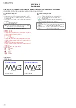
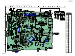
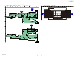
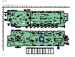
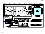
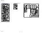
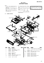
5-3. PRINTED WIRING BOARD – MAIN Section –
•
: Uses unleaded solder.
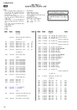
Ref. No. Location
• Semiconductor
Location
D2
F-2
D101
I-2
D102
I-3
D103
I-4
D104
I-3
D105
I-3
D106
I-3
D107
I-2
D108
I-2
D109
I-2
D110
I-2
D114
I-2
D115
I-2
D116
H-3
D301
D-8
D302
C-8
D303
D-8
D304
C-8
D305
C-6
D306
C-6
D307
C-6
D308
C-6
D309
C-6
D310
C-6
D311
C-6
D312
C-7
D400
G-8
D491
E-5
D493
F-7
D494
F-6
D501
I-5
D502
I-5
D511
H-8
D602
F-10
D603
F-10
D604
F-10
D605
B-9
D606
C-9
D607
C-9
D701
C-8
D702
G-9
IC300
B-6
IC401
E-3
IC501
G-6
IC502
H-8
IC601
G-9
IC602
H-8
Q3
F-2
Q420
C-4
Q430
C-3
Q440
C-3
Q460
C-3
Q470
C-4
Q491
E-5
Q492
E-5
Q501
I-6
Q589
I-2
Q590
H-2
Q600
F-10
Q601
G-10
Q605
F-10
Q702
G-10


