25
25
CDX-L480X
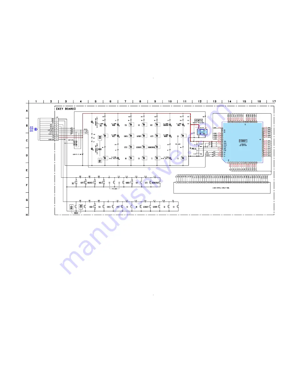
3-12. SCHEMATIC DIAGRAM — KEY SECTION — • Refer to page 18 for Common Note on Schematic Diagram.
Note:
• Voltage is dc with respect to ground under no-signal
(detuned) condition.
no mark : FM
(Page 23)
R901
R902
R903
R911
R912
R913
R991
R981
R982
R983
R984
R985
R986
D901
R972
CN901
R971
R996
R994
R995
R909
R908
R907
R906
R905
R904
R914
R915
R916
R917
R918
R921
R920
R919
R987
R988
R989
LED900
LED901
LED902
LED903
LED906
LED912
LED951
LED952
R931
R932
R933
R941
R942
LSW911(2/2)
LSW910(2/2)
R944
R945
R946
R951
R952
LSW913(2/2)
LSW914(2/2)
LSW915(2/2)
LSW916(2/2)
R954
LSW920(2/2)
R955
LSW919(2/2)
LSW918(2/2)
LSW917(2/2)
R956
R957
LSW907(2/2)
LSW908(2/2)
LSW909(2/2)
LSW921(2/2)
R961
R962
R963
R964
R965
LSW904(2/2)
R966
LSW905(2/2)
R943
C991
C992
C993
C994
C995
C971
R993
R992
S900
S901
S902
S903
LSW905(1/2)
S906
LSW907(1/2)
LSW908(1/2)
LSW909(1/2)
LSW910(1/2)
LSW911(1/2)
S912
LSW913(1/2)
LSW914(1/2)
LSW915(1/2)
LSW916(1/2)
LSW917(1/2)
LSW918(1/2)
LSW919(1/2)
LSW920(1/2)
LSW921(1/2)
LSW904(1/2)
IC971
D991
D902
LED931
LED932
LCD901
IC901


