background image

CMT-SP55TC

AEP Model

UK Model

E Model

SERVICE MANUAL

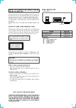
MICRO HI-FI COMPONENT SYSTEM

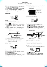
• CMT-SP55TC is composed of following models.

As for the service manual, it is issued for each
component model, then, please refer to it.

 AMPLIFIER CD PLAYER  TAPE DECK    TUNER     SPEAKER SYSTEM

   CMT-SP55TC     TA-SP55

 CDP-SP55

   TC-SP55

  ST-SP55             SS-CSP55

•Abbreviation

AED : North European
MY : Malaysia
SP

: Singapore

KR

: Korea

Part No.

Description

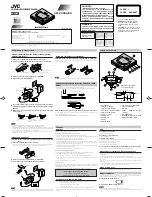
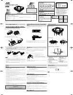
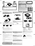
1-476-136-11 REMOTE COMMANDER (RM-SSP55)
1-501-374-11 ANTENNA, LOOP (AM)
1-501-804-11 ANTENNA (FM)(EXCEPT MY, SP)
1-501-659-41 ANTENNA (FM) (MY, SP)
1-792-924-11 CORD (WITH CONNECTOR)(20P)(30cm)

1-792-954-11 CORD, CONNECTION (19P)(40cm)
4-230-235-11 MANUAL, INSTRUCTION (ENGLISH)(AEP, UK, MY, SP)
4-230-235-21 MANUAL, INSTRUCTION (FRENCH, SPANISH)(AEP, MY, SP)
4-230-235-31 MANUAL, INSTRUCTION (GERMAN, DUTCH)(AEP)
4-230-235-41 MANUAL, INSTRUCTION (ITALIAN, PORTUGUESE)(AEP)

4-230-235-51 MANUAL, INSTRUCTION (DANISH, FINNISH, SWEDISH)(AED)
4-230-235-61 MANUAL, INSTRUCTION (CHINESE)(MY, SP)
4-230-235-71 MANUAL, INSTRUCTION (KOREAN)(KR)
4-981-643-21 COVER, BATTERY (FOR RM-SSP55)

PARTS LIST(ACCESSORIES & PACKING MATERIALS)

COMPONENT MODEL NAME FOR CMT-SP55TC

Ver.1.1 2001.03

Sony Corporation

Audio Entertainment Group

General Engineering Dept.

9-929-541-12

2001C0900-1

© 2001. 3

Summary of Contents for CMT-SP55TC

Page 1: ...SP 1 501 659 41 ANTENNA FM MY SP 1 792 924 11 CORD WITH CONNECTOR 20P 30cm 1 792 954 11 CORD CONNECTION 19P 40cm 4 230 235 11 MANUAL INSTRUCTION ENGLISH AEP UK MY SP 4 230 235 21 MANUAL INSTRUCTION FRENCH SPANISH AEP MY SP 4 230 235 31 MANUAL INSTRUCTION GERMAN DUTCH AEP 4 230 235 41 MANUAL INSTRUCTION ITALIAN PORTUGUESE AEP 4 230 235 51 MANUAL INSTRUCTION DANISH FINNISH SWEDISH AED 4 230 235 61 M...

Page 2: ...l E Model General Dimensions w h d Approx 202 75 290 mm Mass Approx 1 5 kg Design and specifications are subject to change without notice System Compact disc and digital audio system Laser Semiconductor laser λ 780 nm Emission duration continuous Laser output Max 44 6 µW This output is the value measured at a distance of 200 mm from the objective lens surface on the Optical Pick up Block with 7 mm...

Page 3: ...ircuit Boards Location 14 5 2 Block Diagram 15 5 3 Printed Wiring Board BD Section 16 5 4 Schematic Diagram BD Section 17 5 5 Printed Wiring Board Main Section 18 5 6 Schematic Diagram Main Section 19 5 7 Printed Wiring Board Loading Section 20 5 8 Schematic Diagram Loading Section 20 5 9 IC Block Diagram 20 6 EXPLODED VIEWS 6 1 Case and Front Panel Section 22 6 2 CD Mechanism Deck Section CDM55C ...

Page 4: ...tential difference generated by the charged electrostatic load etc on clothing and the human body During repair pay attention to electrostatic break down and also use the procedure in the printed matter which is included in the repair parts The flexible board is easily damaged and should be handled with care NOTES ON LASER DIODE EMISSION CHECK The laser beam on this model is concentrated so as to ...

Page 5: ...s CDP together 2 Turn off the unit and reset is executed GC Test Mode Procedure 1 When the power ON press the 1 button TA while pressing the TUNING MODE button ST and PLAY MODE buttons CDP together 2 Fluorescent indicator tube are all turned on 3 Press TUNING MODE button ST to enter the model destination indecation mode SP55 CE2 appears 4 Every pressing of TUNING MODE button ST changes the display...

Page 6: ...set Error History Display Mode Mode for checking the history of errors which have occurred in the CD player Execute this mode after ending the aging mode Procedure 1 Select the function CD using the FUNCTION knob TA 2 While pressing the TUNING MODE button ST and S button CDP press the 1 button TA 3 EMC EDC id displayed Number of mechanism errors Last 3 errors Number of errors NO DISC ERROR which o...

Page 7: ...es 2 Press or to set the hour then press ENTER YES The minute indication flashes 3 Press or to set the minute then press ENTER YES The clock starts If you made a mistake Start over from step 1 To change the preset time You can change the preset time while the system is on 1 Press CLOCK TIMER SET 2 Press or repeatedly until SET CLOCK appears then press ENTER YES 3 Repeat steps 2 and 3 Tips The buil...

Page 8: ... screws case 3 TP2 2 2 3 Set Case Front Panel Assy CD Mechanism Deck CDM55C K6BD38 Holder Assy Optical pick up Main Board Page 8 Cam Gear BD Board Page 9 Page 10 Page 9 Page 8 Page 10 1 connector CN711 4 screw BVTP 3x12 5 front panel assy 2 two screws BVTP 3x12 3 two foot assy s claws claws ...

Page 9: ...8 3 3 CD MECHANISM DECK CDM55C K6BD38 3 4 MAIN BOARD 2 connector CN112 3 screw BVTP 3x8 two claws 5 CD mechanism deck 4 1 flat type wire 19 core CN713 1 screw BVTP 3x8 2 main board ...

Page 10: ...e claw in tne direction of arrow C 0 cam CDM55 3 Pull out the tray 5 bushing C A B B Release 1 Pull out the tray in the arrow direction A and release the lock while pressing this claw in the arrow direction B 2 Remove the Holder BU assy in the direction of arrow A A 1 floating screw PTPWH M2 6 ...

Page 11: ...ICAL PICK UP 3 8 BD BOARD 3 Optical pick up 4 flat type wire 16 core 1 Release the lever in the arrow direction B B 2 sled shaft IC102 IC101 M101 M102 IC103 2 Remove the four solders 1 screw BVTP 2 6x8 3 BD board ...

Page 12: ...P DGND by lead wire 3 Press the 1 button TA 4 Load a disc YEDS 18 and playback 5 Confirm that oscilloscope waveform is clear and check RF signal level is correct or not 6 After check remove the lead wire connected in step 2 BD board Oscilloscope TP FEO TP VC symmetry S curve waveform within 4 1Vp p A B TP RF TP VC BD board oscilloscope Note Clear RF signal waveform means that the shape can be clea...

Page 13: ...12 TP XPCK TP TEO TP FEO TP FEI TP RF TP VC TP DGND TP AGCCON 1 12 24 1 20 21 40 60 80 41 61 IC101 IC103 Adjustment Location BD BOARD Conductor Side ...

Page 14: ... patterns are not indicated U B Line V B Line H adjustment for repair Voltages and waveforms are dc with respect to ground under no signal detuned conditions Voltages are taken with a VOM Input impedance 10 MΩ Voltage variations may be noted due to normal produc tion tolerances Waveforms are taken with a oscilloscope Voltage variations may be noted due to normal produc tion tolerances Circled numb...

Page 15: ...E 6 4Vp p 59nsec 1 2Vp p 2 IC101 ta RFAC PLAY MODE 3 IC101 ra TE PLAY MODE 4 IC101 el FE PLAY MODE 1µsec div approx 300mVp p approx 400mVp p BD BOARD 5 1 CIRCUIT BOARDS LOCATION MAIN board PANEL 1 board PANEL 2 board LOADING board BD board ...

Page 16: ... CLOK CLOCK GENERATOR XTAI R ch XTAO M M TRACKING COIL FOCUS COIL SLED MOTOR M102 SPINDLE MOTOR M101 T T F F SD SD SP SP FOCUS TRACKING COIL DRIVE SPINDLE SLED MOTOR DRIVE IC102 VC TFDR TRDR FFDR FRDR SFDR SRDR XRST MUTE 09 S101 LIMIT SW SQCK XRST SENS SYSTEM CONTROL 2 DATA SCLK XLAT CLOK SCOR SQSO SCOR SQSO SQCK CDMSW HOLD LOAD IN LOAD OUT RF AC ASYI ASYO CONTROL SIGNAL BLOCK SERVO BLOCK VCC VC R...

Page 17: ...CDP SP55 16 16 5 3 PRINTED WIRING BOARD BD SECTION See page 14 for Circuit Boards Location There are a few cases that the part isn t mounted in model is printed on diagram ...

Page 18: ...CDP SP55 17 17 5 4 SCHEMATIC DIAGRAM BD SECTION See page 14 for Waveforms See page 20 for IC Block Diagrams ...

Page 19: ... 14 for Circuit Boards Location There are a few cases that the part isn t mounted in model is printed on diagram Ref No Location D711 A 1 D712 A 1 D713 A 2 D714 A 2 D731 B 4 D741 B 1 IC701 A 1 IC721 A 3 IC731 B 4 IC741 B 1 Q741 B 2 Q742 B 2 Semiconductor Location ...

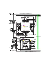
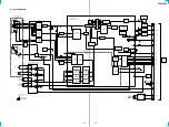
Page 20: ...CDP SP55 19 19 5 6 SCHEMATIC DIAGRAM MAIN SECTION See page 21 for IC Block Diagrams ...

Page 21: ...ATSK SCLK VDD SCOR SPOB XLON XTAI XVDD EMPH AVDD1 AOUT1 AIN1 XTAO XVSS AIN2 AOUT2 AVDD2 RMUT LOUT2 LOUT1 BCK LRCK PCMD LMUT AVSS1 AVSS2 CPU INTERFACE SERVO AUTO SEQUENCER SERIAL IN INTERFACE OVER SAMPLING DIGITAL FILTER 3rd ORDER NOISE SHAPER PWM PWM EFM DEMODULATOR TIMING LOGIC DIGITAL OUT D A INTERFACE DIGITAL PLL ASYMMETRY CORRECTION CLOCK GENERATOR MIRR DFCT FOK DETECTOR DIGITAL CLV SUBCODE PR...

Page 22: ...EF 13 14 15 6 5 1 2 3 4 7 8 9 16 19 20 21 22 23 24 18 17 HOLD LD PD A B C D VEE F E VC AGCVTH AGCCONT VCC LC PD LD_ON HOLD_SW RF_BOT RFTC RF_1 RFO RFE FE TE 50 30 OFF APC PD AMP APC LD AMP IC731 LB1641 MAIN BOARD 1 2 3 4 5 6 7 8 9 10 GND MOTOR DRIVE NOISE FILTER CLAMP FWD IN REV IN VCC 1 VCC 2 NOISE FILTER MOTOR DRIVE MOTOR DRIVE MOTOR DRIVE T S D O C P FWD REV STOP CONTROL LOGIC ...

Page 23: ...a model The components identified by mark 0 or dotted line with mark 0 are critical for safety Replace only with part number specified 1 2 3 4 5 6 7 8 9 2 10 11 12 12 13 14 15 16 not supplied not supplied CDM55C K6BD38 17 18 18 A A 17 17 1 1 678 681 11 PANEL1 BOARD 2 4 951 620 01 SCREW 2 6X8 BVTP 3 4 229 683 01 PLATE R SIDE 4 4 229 678 01 BUTTON U D 5 X 4953 027 1 FOOT ASSY 6 4 229 667 01 PANEL CD...

Page 24: ...504 4 220 239 11 SPRING TORSION 505 4 220 237 01 GEAR A 506 4 221 815 01 ROLLER 507 4 221 816 11 BELT CDM55 508 4 220 233 01 CAM CDM55 509 4 220 234 01 PULLEY LDG 510 4 227 598 01 SPACER 55 511 4 220 238 01 GEAR B 512 1 452 925 21 MAGNET ASSY 513 X 4953 195 1 PULLEY AT ASSY 514 4 985 672 01 SCREW PTPWHM2 6 FLOATING 515 4 227 679 01 INSULATOR 213 516 4 229 806 01 SPRING 213 COMPRESSION 517 X 4953 1...

Page 25: ...A BD BOARD COMPLETE 0552 8 820 116 01 OPTICAL PICK UP KSM 213DCP Z NP 553 1 792 024 11 WIRE FLAT TYPE 16 CORE 554 4 951 620 01 SCREW 2 6X8 BVTP The components identified by mark 0 or dotted line with mark 0 are critical for safety Replace only with part number specified 553 552 554 551 ...

Page 26: ... 180PF 5 50V CONNECTOR CN101 1 784 741 11 CONNECTOR FFC 19P CN102 1 793 907 11 CONNECTOR FFC FPC 16P FERRITE BEAD FB101 1 500 445 21 FERRITE 0UH FB103 1 500 445 21 FERRITE 0UH IC IC101 8 752 386 85 IC CXD2587Q IC102 8 759 549 28 IC BA5974FP E2 IC103 8 752 085 51 IC CXA2568M T6 TRANSISTOR Q101 8 729 049 31 TRANSISTOR 2SB710 RTX RESISTOR R101 1 216 077 91 RES CHIP 15K 5 1 10W R102 1 216 097 11 RES C...

Page 27: ...0V C731 1 161 494 00 CERAMIC 0 022uF 25V C732 1 161 494 00 CERAMIC 0 022uF 25V C741 1 104 664 11 ELECT 47uF 20 00 10V C791 1 104 656 11 ELECT 2200uF 20 00 6 3V C792 1 164 159 11 CERAMIC 0 1uF 50V CONNECTOR CN112 1 568 954 11 PIN CONNECTOR 5P CN701 1 794 498 11 SOCKET CONNECTOR 20P CN711 1 506 469 11 PIN CONNECTOR 4P CN713 1 784 780 11 CONNECTOR FFC 19P DIODE D711 8 719 921 44 DIODE MTZJ T 72 5 1C ...

Page 28: ...ISTOR R776 1 249 437 11 CARBON 47K 5 1 4W R777 1 247 881 00 CARBON 120K 5 1 4W SWITCH S777 1 771 410 21 SWITCH TACTILE REPEAT S778 1 771 410 21 SWITCH TACTILE PLAY MODE MISCELLANEOUS 512 1 452 925 21 MAGNET ASSY 518 1 590 578 11 WIRE FLAT TYPE 19 CORE 0552 8 820 116 01 OPTICAL PICK UP KSM 213DCP Z NP 553 1 792 024 11 WIRE FLAT TYPE 16 CORE M103 A 4672 984 A MOTOR LD ASSY LOADING PANEL 2 PANEL 1 Th...

Page 29: ...ding system 4 track 2 channel stereo Frequency response DOLBY NR OFF 40 14 000 Hz 3 dB using Sony TYPE I cassettes 40 15 000 Hz 3 dB using Sony TYPE II cassettes General Dimensions w h d incl projecting parts and controls Approx 202 x 101 x 283 mm Mass Approx 1 9 kg Supplied accessory System cable 1 Design and specifications are subject to change without notice Ver 1 1 2001 03 Sony Corporation Aud...

Page 30: ...d Panel Section 18 7 6 IC Pin Functions 19 7 7 IC Block Diagrams 20 8 EXPLODED VIEW 8 1 Case and Front Panel 21 9 ELECTRICAL PARTS LIST 22 Abbreviation AED North European model MY Malaysia model SP Singapore model KR Korean model MODEL AEP UK AED models MY SP models KR model PARTS No 4 229 654 0s 4 229 654 2s 4 229 654 3s Parts No SAFETY RELATED COMPONENT WARNING COMPONENTS IDENTIFIED BY MARK 0 OR...

Page 31: ... described above FWD REW Shut off FWD FF AMS FWD REW AMS END Shut off Shut off Cold Reset When the AC cord is removed COLD RESET is done with TC SP55 ST Test Mode Procedure 1 When the power ON press the 1 button TA while pressing the TUNING MODE button ST and PLAY MODE buttons CDP together 2 LCD are all turned on 3 Press TUNING MODE button ST to enter the model destination indecation mode SP55 CE2...

Page 32: ...c Playback of last track 3sec CD tray open CD tray close CD Cassette REW Shut off TAPE AG 1 PLAY FF REV PLAY REW 20 sec TAPE AG 2 20 sec TAPE AG 3 20 sec TAPE AG 4 20 sec TAPE AG 5 FF search REW search OPEN CLOSE 20 sec TAPE AG 6 20 sec TAPE AG 7 TAPE AG 8 TAPE AG 9 6 To end aging execute the cold reset Error History Display Mode Mode for checking the history of errors which have occurred in the C...

Page 33: ... REC indicator 3 z REC button 4 z REC indicator 5 h indicator 6 H indicator 7 S indicator 8 A button 1 4 2 5 6 7 8 9 0 qa qs qd qf qg qh 3 9 M L button q l m button qa s button qs S button qd H button qf h button qg DIRECTION button qh DOLBY NR button ...

Page 34: ...given SECTION 3 DISASSEMBLY Set Case Front Panel Assy Mechanism Assy Page 7 Main Board Page 7 Pinch Roller BLK Assy Belt Page 8 1 two screws case 3 TP2 4 case 1 two screws case 3 TP2 2 2 3 1 connector CN702 4 screw BVTP 3x8 5 front panel assy 2 two screws BVTP 3x12 3 two foot assy s claws claws ...

Page 35: ...M ASSY 3 4 MAIN BOARD 2 two screws BVTP 3x10 3 mechanism assy 2 two screws BVTP 3x10 1 connector CN601 1 connector CN602 1 connector CN101 2 claw 2 claw 1 three screws BVTP 3x8 4 three screws BVTP 3x8 3 5 main board ...

Page 36: ...8 3 5 PINCH ROLLER BLK ASSY BELT 1 two screws belt main F R belt 2 mechanism deck 3 claw 4 pinch roller BLK R assy 6 pinch roller BLK L assy 5 claw 1 two screws 7 belt main 8 F R belt ...

Page 37: ... the test mode either press the 1 button TA and turn OFF the power 4 1 2 TC AGING MODE Procedure 1 After setting the test mode press the H button TC 2 Operations are performed in the following sequence during aging REW Shut off TAPE AG 1 FWD FF REV REW 20 sec TAPE AG 2 20 sec TAPE AG 3 20 sec TAPE AG 4 20 sec 20 sec 20 sec TAPE AG 5 FF search REW search OPEN CLOSE TAPE AG 6 TAPE AG 7 TAPE AG 8 TAP...

Page 38: ... FUNCTION knob TA 3 While pressing the TUNING MODE button ST and H button CDP press the 1 button TA 4 AGING is displayed on the fluorescent display tube briefly 5 Operations are performed in the following sequence during aging Every pressing of DISPLAY button ST changes the display in the CD display and TAPE display Reading of TOC Playback of first track 3sec Playback of last track 3sec CD tray op...

Page 39: ... R CH turn the adjustment screw so that outputs match within 1 dB of peak Record Playback Head Azimuth Adjustment Procedure 1 Mode FWD playback Tape Signal Used for P 4 A100 WS 48B P 4 L300 10 kHz 10 dB 3 kHz 0 dB 315 Hz 0 dB Azimuth Adjustment Tape Speed Adjustment Level Adjustment tast tape P 4 A100 10kHz 10dB set AUX OUT on ST SP55 47kΩ level meter L CH peak R CH peak screw position output leve...

Page 40: ... that adjustment within the following adjustment level Adjustment level AUX OUT level 8 2 0 5 dB 285 to 319 mV Level difference between the channels within 1 0 dB Confirm that the AUX OUT level does not change even though play and stop are repeated Playback Level Adjustment Procedure Mode FWD playback test tape P 4 L300 315Hz 0dB set AUX OUT on ST SP55 level meter Record Bias Adjustment Procedure ...

Page 41: ... R CH on the MAIN board to repeat steps 1 to 3 Adjustment level LINE OUT level 21 8 dB 0 5 dB 59 5 to 66 7 mV Adjustment Location MAIN board AF OSC AUX IN on ST SP55 315Hz 50 mV 23 8 dB blank tape CS 123 set attenuator 600 Ω recorded position set AUX OUT on ST SP55 level meter RV311 L CH RV361 R CH RECORD BIAS RV211 L CH RV261 R CH PB LEVEL RV401 L CH RV451 R CH REC LEVEL TAPE SPEED RV362 RV311 RV...

Page 42: ... indicated U B Line V B Line H adjustment for repair Voltages and waveforms are dc with respect to ground under no signal detuned conditions Voltages are taken with a VOM Input impedance 10 MΩ Voltage variations may be noted due to normal produc tion tolerances Waveforms are taken with a oscilloscope Voltage variations may be noted due to normal produc tion tolerances Circled numbers refer to wave...

Page 43: ...OWN IC603 IC602 IC604 IC605 I2C DATA AGND TC R REC L REC R TC L AGND AGND DGND MGND 7V REG 16 7V 5V 15 3 1 RESET D 5 6V 12V 7V REG 3 1 3 2 7V 1 18 D603 IC702 l m M L s H A h z REC S H h z REC S Q701 705 LED DRIVE D911 D912 CD SYNC REC D913 D914 D915 DOLBY NR DIRECTION CD SYNC REC S911 S910 S909 S908 S907 S906 S905 S904 S903 S902 S901 4 39 38 28 33 40 CAPSTAN MOTOR M LOADING MOTOR M 10 6 2 5 IC601 ...

Page 44: ...16 16 TC SP55 7 2 SCHEMATIC DIAGRAM MAIN SECTION See page 14 for Waveforms See page 19 for IC Pin Functions See page 20 for IC Block Diagrams PIN FUNCTION ...

Page 45: ...601 A 1 D602 A 1 D603 A 4 D604 A 4 D611 C 1 D621 A 5 D622 A 5 D623 A 5 D624 A 5 D701 A 2 IC101 B 6 IC201 C 7 IC401 C 4 IC601 D 2 IC602 A 4 IC603 B 4 IC604 D 6 IC605 B 5 IC701 B 3 IC702 A 2 Q501 D 6 Q502 D 7 Q503 D 7 Q601 C 2 Q602 B 1 Q603 C 2 Q604 B 1 Q701 C 2 Q702 C 2 Q703 C 2 Q704 C 2 Q705 B 2 Semiconductor Location Ref No Location ...

Page 46: ...C DIAGRAM PANEL SECTION 7 5 PRINTED WIRING BOARD PANEL SECTION There are a few cases that the part isn t mounted in model is printed on diagram D911 C 2 D912 C 3 D913 C 4 D914 A 6 D915 A 7 Semiconductor Location Ref No Location ...

Page 47: ...output H OFF L ON 26 REV LED O REV LED control signal output H OFF L ON 27 TC RELAY O Head REC PB select signal output H REC L PB 28 PLAY SW I MC PLAY switch signal input 29 SOL O MC mode exchange solenoid control signal output 30 REC PB PASS I O REC PB PASS select H REC PASS L REC mode 1 2Vcc PB MODE 31 REC MUTE O REC MUTE control H ON L OFF 32 TC MUTE O TC LINE MUTE control signal output H ON L ...

Page 48: ...OCK DIAGRAMS 1 2 3 4 5 6 7 8 9 10 GND MOTOR DRIVE NOISE FILTER CLAMP FWD IN REV IN VCC 1 VCC 2 NOISE FILTER MOTOR DRIVE MOTOR DRIVE MOTOR DRIVE T S D O C P FWD REV STOP CONTROL LOGIC 1 2 3 4 5 6 7 8 9 INVERTER COMPARATER SW R1 GND SW P1 CONT GND VCC SW P2 GND SW R2 ...

Page 49: ...tion Remark 1 1 678 669 11 PANEL BOARD 2 4 951 620 01 SCREW 2 6X8 BVTP 3 4 229 703 01 PLATE R SIDE 4 X 4953 027 1 FOOT ASSY 5 4 229 678 01 BUTTON U D 6 4 229 648 01 PANEL TC FRONT 7 4 229 652 01 INDICATOR PLAY 8 4 229 651 01 INDICATOR REC 9 4 229 704 01 PLATE L SIDE 10 X 4953 025 1 PANEL ASSY TC SUB 11 4 229 653 01 HOLDER TC 12 4 229 649 01 PANEL LOADING 13 A 2004 777 A MECHANISM CMAL2Z720A ASSY 1...

Page 50: ...LECT MELF 10uF 20 50V C406 1 119 820 11 ELECT 1uF 20 50V C407 1 128 854 11 ELECT 0 47uF 20 50V C409 1 137 194 81 FILM 0 47uF 5 50V C410 1 162 290 31 CERAMIC 470PF 10 50V C411 1 126 964 11 ELECT 10uF 20 50V C412 1 126 959 11 ELECT 0 47uF 20 50V C413 1 162 294 31 CERAMIC 0 001uF 10 50V C414 1 126 964 11 ELECT 10uF 20 50V C415 1 126 961 11 ELECT 2 2uF 20 50V C416 1 128 832 11 ELECT 220uF 20 10V C417 ...

Page 51: ... 12K 5 1 4W R362 1 249 433 11 CARBON 22K 5 1 4W R401 1 249 435 11 CARBON 33K 5 1 4W R402 1 249 421 11 CARBON 2 2K 5 1 4W F R405 1 247 807 31 CARBON 100 5 1 4W R406 1 249 429 11 CARBON 10K 5 1 4W R407 1 249 428 11 CARBON 8 2K 5 1 4W F R408 1 249 425 11 CARBON 4 7K 5 1 4W F R409 1 249 433 11 CARBON 22K 5 1 4W R410 1 247 862 11 CARBON 20K 5 1 4W R411 1 247 903 00 CARBON 1M 5 1 4W R412 1 247 884 11 CA...

Page 52: ...1 CARBON 4 7K 5 1 4W F R907 1 249 427 11 CARBON 6 8K 5 1 4W F R908 1 249 429 11 CARBON 10K 5 1 4W R909 1 249 431 11 CARBON 15K 5 1 4W R911 1 249 411 11 CARBON 330 5 1 4W R912 1 249 411 11 CARBON 330 5 1 4W R913 1 249 411 11 CARBON 330 5 1 4W R914 1 249 411 11 CARBON 330 5 1 4W R915 1 249 411 11 CARBON 330 5 1 4W SWITCH S901 1 771 410 21 SWITCH TACTILE z REC S902 1 771 410 21 SWITCH TACTILE CD SYNC...

Page 53: ...m 2 way bass reflex type Speaker units Woofer 12 cm dia glass fiber cone type Tweeter 2 5 cm dia soft dome type Nominal impedance 8 ohms Dimensions w h d incl projecting parts and controls Approx 170 x 275 x230 mm Mass Approx 3 4 kg net per speaker Supplied accessories Speaker cords 2 Design and specification are subject to change without notice ...

Page 54: ...tion Audio Entertainment Group 9 929 534 11 2000H091661 1 Printed in Japan 2000 08 Published by HA Quality Assurance Dept NOTE Items marked are not stocked since they are seldom required for routine service Some delay should be anticipated when ordering these items Hardware mark list and accessories and pack ing materials are given in the last of this parts list 1 2 2 3 4 4 5 4 4 SP101 SP201 not s...

Page 55: ...nals 300 ohms unbalanced Intermediate frequency 10 7 MHz AM tuner section Tuning range European model 531 1 602 kHz with the interval set at 9 kHz Other models 531 1 602 kHz with the interval set at 9 kHz 530 1 710 kHz with the interval set at 10 kHz Aerial AM loop aerial External aerial terminals Intermediate frequency 450 kHz General Dimensions w h d incl projecting parts and controls Approx 202...

Page 56: ...AS SHOWN IN THIS MANUAL OR IN SUPPLEMENTS PUBLISHED BY SONY TABLE OF CONTENTS 1 SERVICE NOTE 3 2 GENERAL 3 3 DIAGRAMS 3 1 Circuit Boards Location 4 3 2 Block Diagram 5 3 3 Schematic Diagram Main Section 6 3 4 Printed Wiring Board Main Section 7 3 5 Schematic Diagram Panel Section 8 3 6 Printed Wiring Board Panel Section 9 3 7 IC Pin Functions 10 3 8 IC Block Diagram 11 4 EXPLODED VIEW 4 1 Case and...

Page 57: ...utton ST and lm buttons CDP together 2 Turn off the unit and reset is executed GC Test Mode Procedure 1 When the power ON press the 1 button TA while pressing the TUNING MODE button ST and PLAY MODE buttons CDP together 2 LCD are all turned on 3 Press TUNING MODE button ST to enter the model destination indecation mode SP55 CE2 or SP55 ASIA2 appears 4 Every pressing of TUNING MODE button ST change...

Page 58: ...justment for repair no mark FM Can not be measured Voltages are taken with a VOM Input impedance 10 MΩ Voltage variations may be noted due to normal produc tion tolerances Waveforms are taken with a oscilloscope Voltage variations may be noted due to normal produc tion tolerances Circled numbers refer to waveforms Signal path F FM J CD d TAPE G REC TAPE MD j MD Abbreviation MY Malaysia model SP Si...

Page 59: ...DKEY PLAY LED PAUSE LED DATA XLAT CLOK HOLD SQSO SENS SQCK SCOR CD MSW LOAD IN LOAD OUT CD KEY LED0 LED1 CD DATA CD XLAT CD CLK HOLD SQSO SENS SQCK SCOR CDM SW CD PWR UBREG L LOAD IN LOAD OUT UNREG L 5V SYSTEM CONTROL 2 TO CDP SP55 SYSTEM CONTROL 1 FROM TA SP55 SYSTEM CONTROL 3 SYSTEM CONTROL 3 TO TC SP55 MDS SP55 TO TC SP55 MDS SP55 CN203 1 2 J210 2 2 CN203 2 2 CN201 J210 1 2 CN205 UNREG L UNREG ...

Page 60: ...ST SP55 6 6 3 3 SCHEMATIC DIAGRAM MAIN SECTION Page 8 Page 8 Page 8 PIN FUNCTION ...

Page 61: ...ocation D201 D 5 D282 E 6 D283 G 6 D291 E 4 D301 F 5 D701 F 3 D702 F 3 D731 C 2 D733 C 3 IC202 B 4 IC231 A 6 IC281 G 6 IC282 G 7 IC283 F 5 IC401 C 5 IC701 E 2 IC702 C 3 Q201 B 3 Q221 A 6 Q271 A 5 Q281 A 7 Q282 A 6 Q291 F 4 Q301 F 5 Q701 G 3 Q702 F 1 Q704 G 3 Q705 F 2 Q706 F 2 Q731 B 3 Semiconductor Location Page 9 Page 9 Page 9 AEP UK AED ...

Page 62: ...ST SP55 8 8 3 5 SCHEMATIC DIAGRAM PANEL SECTION Page 6 Page 6 Page 6 LCD BACK LIGHT ...

Page 63: ...ST SP55 9 9 3 6 PRINTED WIRING BOARD PANEL SECTION There are a few cases that the part isn t mounted in model is printed on diagram Page 7 Page 7 Page 7 ...

Page 64: ...51 RO_MUTE_AUX O AUX out mute signal output H MUTE OFF L MUTE 52 to 57 N C Not used 58 FUNC_INHIBIT O TA input select inhibit signal H INHIBIT L NOT INHIBIT 59 N C O Not used 60 FUNC2 O TA input select signal output 61 FUNC1 O TA input select signal output 62 VCC Power Supply EVER 5V 63 N C Not used Function Pin Name Pin No 3 7 IC PIN FUNCTIONS IC701 M30620MCA A67FP MASTER CONTROL MAIN BOARD 64 VS...

Page 65: ...18 19 20 LOGIC CIRCUIT CCB INTERFACE CONTROL CIRCUIT 1 2 4 28 29 27 3 30 5 6 7 CONTROL CIRCUIT 8 9 10 21 22 23 24 25 26 LOUT LBASS2 LBASS1 LTRE LIN LSELO RROUT RBASS2 RBASS1 RTRE RIN RSELO L4 L3 L2 L1 NC NC R1 R2 R3 R4 LVREF RVREF TEST TVSS CE DI CL VDD VREF NC ...

Page 66: ...L ST FRONT HK MY SP KR 9 4 229 684 01 PLATE L SIDE 10 X 4953 022 1 PANEL ASSY ST SUB 11 4 229 680 01 ILLUMINATOR 12 4 229 679 01 HOLDER LCD 13 1 678 672 11 LED BOARD 14 1 769 970 11 WIRE FLAT TYPE 13 CORE HK MY SP KR 14 1 773 002 11 WIRE FLAT TYPE 15 CORE AEP UK AED Ref No Part No Description Remarks Ref No Part No Description Remarks 15 A 4424 804 A MAIN BOARD COMPLETE AEP UK AED 15 A 4473 725 A ...

Page 67: ...MELF 2 2uF 20 50V C267 1 130 476 00 MYLAR 0 0027uF 5 50V C268 1 136 177 00 MYLAR 1uF 5 50V C269 1 136 177 00 MYLAR 1uF 5 50V C270 1 119 820 11 ELECT 1uF 20 50V C275 1 162 282 31 CERAMIC 100PF 10 50V C278 1 162 294 31 CERAMIC 0 001uF 10 50V C281 1 128 547 11 ELECT 6800uF 20 16V C282 1 126 936 11 ELECT 3300uF 20 16V C283 1 161 494 00 CERAMIC 0 022uF 25V C284 1 161 494 00 CERAMIC 0 022uF 25V C285 1 1...

Page 68: ...ON 4 7K 5 1 4W F R212 1 249 429 11 CARBON 10K 5 1 4W R213 1 249 418 11 CARBON 1 2K 5 1 4W F R214 1 249 429 11 CARBON 10K 5 1 4W R215 1 249 421 11 CARBON 2 2K 5 1 4W F R216 1 249 429 11 CARBON 10K 5 1 4W R217 1 249 417 11 CARBON 1K 5 1 4W F R218 1 247 843 11 CARBON 3 3K 5 1 4W R219 1 249 393 11 CARBON 10 5 1 4W F R221 1 249 421 11 CARBON 2 2K 5 1 4W F R222 1 249 429 11 CARBON 10K 5 1 4W R223 1 249 ...

Page 69: ...7 807 31 CARBON 100 5 1 4W R778 1 249 401 11 CARBON 47 5 1 4W F R779 1 249 401 11 CARBON 47 5 1 4W F VIBRATOR X701 1 579 175 11 VIBRATOR CERAMIC 10MHz X702 1 567 098 41 VIBRATOR CRYSTAL 32 768KHz 1 678 671 11 PANEL BOARD CAPACITOR C901 1 124 584 00 ELECT 100uF 20 10V C902 1 161 494 00 CERAMIC 0 022uF 25V C903 1 161 494 00 CERAMIC 0 022uF 25V C904 1 162 290 31 CERAMIC 470PF 10 50V C905 1 162 290 31...

Page 70: ... No Part No Description Remarks Ref No Part No Description Remarks ST SP55 Sony Corporation Audio Entertainment Group 9 929 536 11 2000I097551 1 Printed in Hungary 2000 9 Published by General Engineering Dept ...

Page 71: ...ding system 4 track 2 channel stereo Frequency response DOLBY NR OFF 40 14 000 Hz 3 dB using Sony TYPE I cassettes 40 15 000 Hz 3 dB using Sony TYPE II cassettes General Dimensions w h d incl projecting parts and controls Approx 202 x 101 x 283 mm Mass Approx 1 9 kg Supplied accessory System cable 1 Design and specifications are subject to change without notice Ver 1 1 2001 03 Sony Corporation Aud...

Page 72: ...d Panel Section 18 7 6 IC Pin Functions 19 7 7 IC Block Diagrams 20 8 EXPLODED VIEW 8 1 Case and Front Panel 21 9 ELECTRICAL PARTS LIST 22 Abbreviation AED North European model MY Malaysia model SP Singapore model KR Korean model MODEL AEP UK AED models MY SP models KR model PARTS No 4 229 654 0s 4 229 654 2s 4 229 654 3s Parts No SAFETY RELATED COMPONENT WARNING COMPONENTS IDENTIFIED BY MARK 0 OR...

Page 73: ... described above FWD REW Shut off FWD FF AMS FWD REW AMS END Shut off Shut off Cold Reset When the AC cord is removed COLD RESET is done with TC SP55 ST Test Mode Procedure 1 When the power ON press the 1 button TA while pressing the TUNING MODE button ST and PLAY MODE buttons CDP together 2 LCD are all turned on 3 Press TUNING MODE button ST to enter the model destination indecation mode SP55 CE2...

Page 74: ...c Playback of last track 3sec CD tray open CD tray close CD Cassette REW Shut off TAPE AG 1 PLAY FF REV PLAY REW 20 sec TAPE AG 2 20 sec TAPE AG 3 20 sec TAPE AG 4 20 sec TAPE AG 5 FF search REW search OPEN CLOSE 20 sec TAPE AG 6 20 sec TAPE AG 7 TAPE AG 8 TAPE AG 9 6 To end aging execute the cold reset Error History Display Mode Mode for checking the history of errors which have occurred in the C...

Page 75: ... REC indicator 3 z REC button 4 z REC indicator 5 h indicator 6 H indicator 7 S indicator 8 A button 1 4 2 5 6 7 8 9 0 qa qs qd qf qg qh 3 9 M L button q l m button qa s button qs S button qd H button qf h button qg DIRECTION button qh DOLBY NR button ...

Page 76: ...given SECTION 3 DISASSEMBLY Set Case Front Panel Assy Mechanism Assy Page 7 Main Board Page 7 Pinch Roller BLK Assy Belt Page 8 1 two screws case 3 TP2 4 case 1 two screws case 3 TP2 2 2 3 1 connector CN702 4 screw BVTP 3x8 5 front panel assy 2 two screws BVTP 3x12 3 two foot assy s claws claws ...

Page 77: ...M ASSY 3 4 MAIN BOARD 2 two screws BVTP 3x10 3 mechanism assy 2 two screws BVTP 3x10 1 connector CN601 1 connector CN602 1 connector CN101 2 claw 2 claw 1 three screws BVTP 3x8 4 three screws BVTP 3x8 3 5 main board ...

Page 78: ...8 3 5 PINCH ROLLER BLK ASSY BELT 1 two screws belt main F R belt 2 mechanism deck 3 claw 4 pinch roller BLK R assy 6 pinch roller BLK L assy 5 claw 1 two screws 7 belt main 8 F R belt ...

Page 79: ... the test mode either press the 1 button TA and turn OFF the power 4 1 2 TC AGING MODE Procedure 1 After setting the test mode press the H button TC 2 Operations are performed in the following sequence during aging REW Shut off TAPE AG 1 FWD FF REV REW 20 sec TAPE AG 2 20 sec TAPE AG 3 20 sec TAPE AG 4 20 sec 20 sec 20 sec TAPE AG 5 FF search REW search OPEN CLOSE TAPE AG 6 TAPE AG 7 TAPE AG 8 TAP...

Page 80: ... FUNCTION knob TA 3 While pressing the TUNING MODE button ST and H button CDP press the 1 button TA 4 AGING is displayed on the fluorescent display tube briefly 5 Operations are performed in the following sequence during aging Every pressing of DISPLAY button ST changes the display in the CD display and TAPE display Reading of TOC Playback of first track 3sec Playback of last track 3sec CD tray op...

Page 81: ... R CH turn the adjustment screw so that outputs match within 1 dB of peak Record Playback Head Azimuth Adjustment Procedure 1 Mode FWD playback Tape Signal Used for P 4 A100 WS 48B P 4 L300 10 kHz 10 dB 3 kHz 0 dB 315 Hz 0 dB Azimuth Adjustment Tape Speed Adjustment Level Adjustment tast tape P 4 A100 10kHz 10dB set AUX OUT on ST SP55 47kΩ level meter L CH peak R CH peak screw position output leve...

Page 82: ... that adjustment within the following adjustment level Adjustment level AUX OUT level 8 2 0 5 dB 285 to 319 mV Level difference between the channels within 1 0 dB Confirm that the AUX OUT level does not change even though play and stop are repeated Playback Level Adjustment Procedure Mode FWD playback test tape P 4 L300 315Hz 0dB set AUX OUT on ST SP55 level meter Record Bias Adjustment Procedure ...

Page 83: ... R CH on the MAIN board to repeat steps 1 to 3 Adjustment level LINE OUT level 21 8 dB 0 5 dB 59 5 to 66 7 mV Adjustment Location MAIN board AF OSC AUX IN on ST SP55 315Hz 50 mV 23 8 dB blank tape CS 123 set attenuator 600 Ω recorded position set AUX OUT on ST SP55 level meter RV311 L CH RV361 R CH RECORD BIAS RV211 L CH RV261 R CH PB LEVEL RV401 L CH RV451 R CH REC LEVEL TAPE SPEED RV362 RV311 RV...

Page 84: ... indicated U B Line V B Line H adjustment for repair Voltages and waveforms are dc with respect to ground under no signal detuned conditions Voltages are taken with a VOM Input impedance 10 MΩ Voltage variations may be noted due to normal produc tion tolerances Waveforms are taken with a oscilloscope Voltage variations may be noted due to normal produc tion tolerances Circled numbers refer to wave...

Page 85: ...OWN IC603 IC602 IC604 IC605 I2C DATA AGND TC R REC L REC R TC L AGND AGND DGND MGND 7V REG 16 7V 5V 15 3 1 RESET D 5 6V 12V 7V REG 3 1 3 2 7V 1 18 D603 IC702 l m M L s H A h z REC S H h z REC S Q701 705 LED DRIVE D911 D912 CD SYNC REC D913 D914 D915 DOLBY NR DIRECTION CD SYNC REC S911 S910 S909 S908 S907 S906 S905 S904 S903 S902 S901 4 39 38 28 33 40 CAPSTAN MOTOR M LOADING MOTOR M 10 6 2 5 IC601 ...

Page 86: ...16 16 TC SP55 7 2 SCHEMATIC DIAGRAM MAIN SECTION See page 14 for Waveforms See page 19 for IC Pin Functions See page 20 for IC Block Diagrams PIN FUNCTION ...

Page 87: ...601 A 1 D602 A 1 D603 A 4 D604 A 4 D611 C 1 D621 A 5 D622 A 5 D623 A 5 D624 A 5 D701 A 2 IC101 B 6 IC201 C 7 IC401 C 4 IC601 D 2 IC602 A 4 IC603 B 4 IC604 D 6 IC605 B 5 IC701 B 3 IC702 A 2 Q501 D 6 Q502 D 7 Q503 D 7 Q601 C 2 Q602 B 1 Q603 C 2 Q604 B 1 Q701 C 2 Q702 C 2 Q703 C 2 Q704 C 2 Q705 B 2 Semiconductor Location Ref No Location ...

Page 88: ...C DIAGRAM PANEL SECTION 7 5 PRINTED WIRING BOARD PANEL SECTION There are a few cases that the part isn t mounted in model is printed on diagram D911 C 2 D912 C 3 D913 C 4 D914 A 6 D915 A 7 Semiconductor Location Ref No Location ...

Page 89: ...output H OFF L ON 26 REV LED O REV LED control signal output H OFF L ON 27 TC RELAY O Head REC PB select signal output H REC L PB 28 PLAY SW I MC PLAY switch signal input 29 SOL O MC mode exchange solenoid control signal output 30 REC PB PASS I O REC PB PASS select H REC PASS L REC mode 1 2Vcc PB MODE 31 REC MUTE O REC MUTE control H ON L OFF 32 TC MUTE O TC LINE MUTE control signal output H ON L ...

Page 90: ...OCK DIAGRAMS 1 2 3 4 5 6 7 8 9 10 GND MOTOR DRIVE NOISE FILTER CLAMP FWD IN REV IN VCC 1 VCC 2 NOISE FILTER MOTOR DRIVE MOTOR DRIVE MOTOR DRIVE T S D O C P FWD REV STOP CONTROL LOGIC 1 2 3 4 5 6 7 8 9 INVERTER COMPARATER SW R1 GND SW P1 CONT GND VCC SW P2 GND SW R2 ...

Page 91: ...tion Remark 1 1 678 669 11 PANEL BOARD 2 4 951 620 01 SCREW 2 6X8 BVTP 3 4 229 703 01 PLATE R SIDE 4 X 4953 027 1 FOOT ASSY 5 4 229 678 01 BUTTON U D 6 4 229 648 01 PANEL TC FRONT 7 4 229 652 01 INDICATOR PLAY 8 4 229 651 01 INDICATOR REC 9 4 229 704 01 PLATE L SIDE 10 X 4953 025 1 PANEL ASSY TC SUB 11 4 229 653 01 HOLDER TC 12 4 229 649 01 PANEL LOADING 13 A 2004 777 A MECHANISM CMAL2Z720A ASSY 1...

Page 92: ...LECT MELF 10uF 20 50V C406 1 119 820 11 ELECT 1uF 20 50V C407 1 128 854 11 ELECT 0 47uF 20 50V C409 1 137 194 81 FILM 0 47uF 5 50V C410 1 162 290 31 CERAMIC 470PF 10 50V C411 1 126 964 11 ELECT 10uF 20 50V C412 1 126 959 11 ELECT 0 47uF 20 50V C413 1 162 294 31 CERAMIC 0 001uF 10 50V C414 1 126 964 11 ELECT 10uF 20 50V C415 1 126 961 11 ELECT 2 2uF 20 50V C416 1 128 832 11 ELECT 220uF 20 10V C417 ...

Page 93: ... 12K 5 1 4W R362 1 249 433 11 CARBON 22K 5 1 4W R401 1 249 435 11 CARBON 33K 5 1 4W R402 1 249 421 11 CARBON 2 2K 5 1 4W F R405 1 247 807 31 CARBON 100 5 1 4W R406 1 249 429 11 CARBON 10K 5 1 4W R407 1 249 428 11 CARBON 8 2K 5 1 4W F R408 1 249 425 11 CARBON 4 7K 5 1 4W F R409 1 249 433 11 CARBON 22K 5 1 4W R410 1 247 862 11 CARBON 20K 5 1 4W R411 1 247 903 00 CARBON 1M 5 1 4W R412 1 247 884 11 CA...

Page 94: ...1 CARBON 4 7K 5 1 4W F R907 1 249 427 11 CARBON 6 8K 5 1 4W F R908 1 249 429 11 CARBON 10K 5 1 4W R909 1 249 431 11 CARBON 15K 5 1 4W R911 1 249 411 11 CARBON 330 5 1 4W R912 1 249 411 11 CARBON 330 5 1 4W R913 1 249 411 11 CARBON 330 5 1 4W R914 1 249 411 11 CARBON 330 5 1 4W R915 1 249 411 11 CARBON 330 5 1 4W SWITCH S901 1 771 410 21 SWITCH TACTILE z REC S902 1 771 410 21 SWITCH TACTILE CD SYNC...

Page 95: ...eral Power requirements European model 230 V AC 50 60 Hz Other models 110 120 V or 220 240 V AC 50 60 Hz Power consumption 70 watts Dimensions w h d Mass Approx Approx 202 x 101 x 306 mm 3 9 kg Design and specifications are subject to change without notice Other models DIN power output Rated 25 25 watts 8 ohms at 1 kHz DIN 240 V 22 22 watts 8 ohms at 1 kHz DIN 220 V Continuous RMS power output Ref...

Page 96: ...ssy 5 3 3 HP Board Panel Board 6 4 DIAGRAMS 4 1 Block Diagram 9 4 2 Printed Wiring Board Main Section 10 4 3 Schematic Diagram Main Section 11 4 4 Printed Wiring Board Panel Section 12 4 5 Schematic Diagram Panel Section 13 4 6 Printed Wiring Board VOLSEL Section 14 5 EXPLODED VIEWS 5 1 Case and Front Panel 15 6 ELECTRICAL PARTS LIST 16 MODEL IDENTIFICATION MODEL PARTS No AEP AED UK model 4 229 70...

Page 97: ...SPLAY button ST changes the display in the Version display and model destination display 6 Press TUNER BAND button ST to enter the key check mode 7 In the key check mode the fluorescent indicator tube displays Key 0 Vol 0 Each time a button is pressed Key value increases However once a button is pressed it is no longer taken into account Vol Value increases like 1 2 3 if rotating VOLUME knob TA in...

Page 98: ...to set the minute then press ENTER YES The clock starts If you made a mistake Start over from step 1 To change the preset time You can change the preset time while the system is on 1 Press CLOCK TIMER SET 2 Press or repeatedly until SET CLOCK appears then press ENTER YES 3 Repeat steps 2 and 3 Tips The built in clock shows the time in the display while the system is off If you press DISPLAY at thi...

Page 99: ...NT PANEL ASSY Set Case Front Panel Assy HP Board Panel Board 1 two screws case 3 TP2 4 case 1 two screws case 3 TP2 2 2 3 1 flat type wire 17 core CN303 4 screw BVTP 3x12 5 front panel assy 2 two screws BVTP 3x12 3 two foot assy s claws claws ...

Page 100: ...3 HP BOARD PANEL BOARD 0 three screws BVTP 2 6x8 qa panel board 0 screw BVTP 2 6x8 1 panel L side 5 HP board 6 two knobs DSG 8 nut 7 knobs VOL 9 knobs select 3 panel TA front 4 1 panel R side 2 claw 2 claw ...

Page 101: ...djustment for repair Voltages and waveforms are dc with respect to ground under no signal detuned conditions Voltages are taken with a VOM Input impedance 10 MΩ Voltage variations may be noted due to normal produc tion tolerances Waveforms are taken with a oscilloscope Voltage variations may be noted due to normal produc tion tolerances Signal path K FM Abbreviation AED North European model MY Mal...

Page 102: ...8 MEMO ...

Page 103: ...AED UK KR model JW104 IC502 JW101 AEP AED UK KR model Q211 AC IN L L SPEAKER PHONE TM801 R CH R CH R CH R CH IC801 POWER AMP Q512 Q314 MUTE A IC552 2 2 IC552 1 2 Q301 302 BUFFER Q516 IC501 SHK PROCESSOR TREB BASS L SHK TREBLE RV503 RV502 BASS L R UNREG L UNREG L 5 6V UNSW 13V REG XPRE MUTE HP MUTE XS RELAY P RELAY DSG OFF TA KEY HPSW ON STBY AMP MUTE ENC0 ENC1 ENC0 ENC1 R CH L ORG UNREG L UNREG L ...

Page 104: ...D205 C 2 D206 C 2 D207 B 5 D208 B 5 D209 D 5 D210 D 5 D211 F 4 D212 F 4 D213 F 4 D214 F 4 D215 E 4 D216 F 5 D217 B 1 D218 D 4 D251 B 6 D311 A 4 D551 A 7 D553 B 9 D554 B 9 D821 A 7 IC211 E 4 IC801 E 7 Q201 C 1 Q202 B 3 Q211 E 4 Q301 B 2 Q302 B 2 Q311 A 4 Q312 C 5 Q313 A 3 Q314 B 3 Q315 A 3 Q512 B 3 Q552 B 9 Q553 B 8 Q562 B 3 Q801 A 7 Q802 A 8 Q803 A 8 Q804 A 7 Semiconductor Location 12 ...

Page 105: ...TA SP55 11 11 4 3 SCHEMATIC DIAGRAM MAIN SECTION ...

Page 106: ...SECTION There are a few cases that the part isn t mounted in model is printed on diagram Ref No Location D522 B 2 D523 B 2 D911 B 5 D912 A 7 IC501 B 5 IC502 B 4 IC522 B 2 Q511 A 4 Q561 A 4 Q911 A 6 Q912 A 6 Q913 A 6 Q914 A 6 Semiconductor Location ...

Page 107: ...TA SP55 13 13 4 5 SCHEMATIC DIAGRAM PANEL SECTION ...

Page 108: ...TA SP55 14 14 4 6 PRINTED WIRING BOARD VOLSEL SECTION There are a few cases that the part isn t mounted in model is printed on diagram ...

Page 109: ...4 229 693 01 KNOB DSG 9 4 229 690 01 PANEL TA FRONT 10 4 229 697 01 INDICATOR P 11 4 229 704 01 PLATE L SIDE 12 X 4953 023 1 PANEL ASSY TA SUB 13 1 678 678 11 HP BOARD 14 4 900 386 01 SCREW 15 3 363 099 51 SCREW CASE 3 TP2 16 4 229 701 31 CASE 17 A 4473 728 A MAIN BOARD COMPLETE AEP AED UK KR 17 A 4473 732 A MAIN BOARD COMPLETE HK MY SP 18 3 970 608 11 SUMITITE B3 BV 019 1 769 079 11 CORD POWER KR...

Page 110: ... 1 164 159 11 CERAMIC 0 1uF 50V C823 1 162 219 31 CERAMIC 68PF 5 50V C824 1 164 159 11 CERAMIC 0 1uF 50V C825 1 164 159 11 CERAMIC 0 1uF 50V C850 1 164 159 11 CERAMIC 0 1uF 50V C861 1 161 494 00 CERAMIC 0 022uF 25V C862 1 161 494 00 CERAMIC 0 022uF 25V C863 1 164 159 11 CERAMIC 0 1uF 50V C873 1 162 219 31 CERAMIC 68PF 5 50V C874 1 164 159 11 CERAMIC 0 1uF 50V C875 1 164 159 11 CERAMIC 0 1uF 50V C8...

Page 111: ...4W R202 1 247 843 11 CARBON 3 3K 5 1 4W R211 1 249 429 11 CARBON 10K 5 1 4W R213 1 249 429 11 CARBON 10K 5 1 4W R303 1 247 807 31 CARBON 100 5 1 4W R304 1 247 807 31 CARBON 100 5 1 4W R305 1 247 807 31 CARBON 100 5 1 4W R306 1 247 807 31 CARBON 100 5 1 4W R311 1 249 413 11 CARBON 470 5 1 4W F R312 1 249 413 11 CARBON 470 5 1 4W F R313 1 249 441 11 CARBON 100K 5 1 4W R501 1 247 843 11 CARBON 3 3K 5...

Page 112: ... 1 249 425 11 CARBON 4 7K 5 1 4W F R513 1 249 433 11 CARBON 22K 5 1 4W R516 1 249 429 11 CARBON 10K 5 1 4W R520 1 249 409 11 CARBON 220 5 1 4W F R521 1 249 409 11 CARBON 220 5 1 4W F R522 1 249 429 11 CARBON 10K 5 1 4W R523 1 249 429 11 CARBON 10K 5 1 4W R524 1 249 429 11 CARBON 10K 5 1 4W R525 1 249 429 11 CARBON 10K 5 1 4W R526 1 249 441 11 CARBON 100K 5 1 4W R527 1 249 429 11 CARBON 10K 5 1 4W ...

Page 113: ...777 071 61 CORD POWER AEP AED UK HK MY SP 21 1 792 922 11 CORD WITH CONNECTOR 25 1 500 386 11 FILTER CLAMP FERRITE CORE M101 1 698 997 21 FAN D C 0T102 1 435 600 11 TRANSFORMER POWER AEP AED UK KR 0T102 1 435 601 11 TRANSFORMER POWER HK MY SP ACCESSORIES PACKING MATERIALS 0 1 569 008 21 ADAPTOR CONVERSION 2P MY SP 0 1 770 019 11 ADAPTOR CONVERSION PLUG 3P UK HK ...

Page 114: ... No Part No Description Remarks Ref No Part No Description Remarks TA SP55 Sony Corporation Audio Entertainment Group 9 929 535 11 2000I097551 1 Printed in Hungary 2000 9 Published by General Engineering Dept ...

Page 115: ...l E Model General Dimensions w h d Approx 202 75 290 mm Mass Approx 1 5 kg Design and specifications are subject to change without notice System Compact disc and digital audio system Laser Semiconductor laser λ 780 nm Emission duration continuous Laser output Max 44 6 µW This output is the value measured at a distance of 200 mm from the objective lens surface on the Optical Pick up Block with 7 mm...

Page 116: ...ircuit Boards Location 14 5 2 Block Diagram 15 5 3 Printed Wiring Board BD Section 16 5 4 Schematic Diagram BD Section 17 5 5 Printed Wiring Board Main Section 18 5 6 Schematic Diagram Main Section 19 5 7 Printed Wiring Board Loading Section 20 5 8 Schematic Diagram Loading Section 20 5 9 IC Block Diagram 20 6 EXPLODED VIEWS 6 1 Case and Front Panel Section 22 6 2 CD Mechanism Deck Section CDM55C ...

Page 117: ...tential difference generated by the charged electrostatic load etc on clothing and the human body During repair pay attention to electrostatic break down and also use the procedure in the printed matter which is included in the repair parts The flexible board is easily damaged and should be handled with care NOTES ON LASER DIODE EMISSION CHECK The laser beam on this model is concentrated so as to ...

Page 118: ...s CDP together 2 Turn off the unit and reset is executed GC Test Mode Procedure 1 When the power ON press the 1 button TA while pressing the TUNING MODE button ST and PLAY MODE buttons CDP together 2 Fluorescent indicator tube are all turned on 3 Press TUNING MODE button ST to enter the model destination indecation mode SP55 CE2 appears 4 Every pressing of TUNING MODE button ST changes the display...

Page 119: ...set Error History Display Mode Mode for checking the history of errors which have occurred in the CD player Execute this mode after ending the aging mode Procedure 1 Select the function CD using the FUNCTION knob TA 2 While pressing the TUNING MODE button ST and S button CDP press the 1 button TA 3 EMC EDC id displayed Number of mechanism errors Last 3 errors Number of errors NO DISC ERROR which o...

Page 120: ...es 2 Press or to set the hour then press ENTER YES The minute indication flashes 3 Press or to set the minute then press ENTER YES The clock starts If you made a mistake Start over from step 1 To change the preset time You can change the preset time while the system is on 1 Press CLOCK TIMER SET 2 Press or repeatedly until SET CLOCK appears then press ENTER YES 3 Repeat steps 2 and 3 Tips The buil...

Page 121: ... screws case 3 TP2 2 2 3 Set Case Front Panel Assy CD Mechanism Deck CDM55C K6BD38 Holder Assy Optical pick up Main Board Page 8 Cam Gear BD Board Page 9 Page 10 Page 9 Page 8 Page 10 1 connector CN711 4 screw BVTP 3x12 5 front panel assy 2 two screws BVTP 3x12 3 two foot assy s claws claws ...

Page 122: ...8 3 3 CD MECHANISM DECK CDM55C K6BD38 3 4 MAIN BOARD 2 connector CN112 3 screw BVTP 3x8 two claws 5 CD mechanism deck 4 1 flat type wire 19 core CN713 1 screw BVTP 3x8 2 main board ...

Page 123: ...e claw in tne direction of arrow C 0 cam CDM55 3 Pull out the tray 5 bushing C A B B Release 1 Pull out the tray in the arrow direction A and release the lock while pressing this claw in the arrow direction B 2 Remove the Holder BU assy in the direction of arrow A A 1 floating screw PTPWH M2 6 ...

Page 124: ...ICAL PICK UP 3 8 BD BOARD 3 Optical pick up 4 flat type wire 16 core 1 Release the lever in the arrow direction B B 2 sled shaft IC102 IC101 M101 M102 IC103 2 Remove the four solders 1 screw BVTP 2 6x8 3 BD board ...

Page 125: ...P DGND by lead wire 3 Press the 1 button TA 4 Load a disc YEDS 18 and playback 5 Confirm that oscilloscope waveform is clear and check RF signal level is correct or not 6 After check remove the lead wire connected in step 2 BD board Oscilloscope TP FEO TP VC symmetry S curve waveform within 4 1Vp p A B TP RF TP VC BD board oscilloscope Note Clear RF signal waveform means that the shape can be clea...

Page 126: ...12 TP XPCK TP TEO TP FEO TP FEI TP RF TP VC TP DGND TP AGCCON 1 12 24 1 20 21 40 60 80 41 61 IC101 IC103 Adjustment Location BD BOARD Conductor Side ...

Page 127: ... patterns are not indicated U B Line V B Line H adjustment for repair Voltages and waveforms are dc with respect to ground under no signal detuned conditions Voltages are taken with a VOM Input impedance 10 MΩ Voltage variations may be noted due to normal produc tion tolerances Waveforms are taken with a oscilloscope Voltage variations may be noted due to normal produc tion tolerances Circled numb...

Page 128: ...E 6 4Vp p 59nsec 1 2Vp p 2 IC101 ta RFAC PLAY MODE 3 IC101 ra TE PLAY MODE 4 IC101 el FE PLAY MODE 1µsec div approx 300mVp p approx 400mVp p BD BOARD 5 1 CIRCUIT BOARDS LOCATION MAIN board PANEL 1 board PANEL 2 board LOADING board BD board ...

Page 129: ... CLOK CLOCK GENERATOR XTAI R ch XTAO M M TRACKING COIL FOCUS COIL SLED MOTOR M102 SPINDLE MOTOR M101 T T F F SD SD SP SP FOCUS TRACKING COIL DRIVE SPINDLE SLED MOTOR DRIVE IC102 VC TFDR TRDR FFDR FRDR SFDR SRDR XRST MUTE 09 S101 LIMIT SW SQCK XRST SENS SYSTEM CONTROL 2 DATA SCLK XLAT CLOK SCOR SQSO SCOR SQSO SQCK CDMSW HOLD LOAD IN LOAD OUT RF AC ASYI ASYO CONTROL SIGNAL BLOCK SERVO BLOCK VCC VC R...

Page 130: ...CDP SP55 16 16 5 3 PRINTED WIRING BOARD BD SECTION See page 14 for Circuit Boards Location There are a few cases that the part isn t mounted in model is printed on diagram ...

Page 131: ...CDP SP55 17 17 5 4 SCHEMATIC DIAGRAM BD SECTION See page 14 for Waveforms See page 20 for IC Block Diagrams ...

Page 132: ... 14 for Circuit Boards Location There are a few cases that the part isn t mounted in model is printed on diagram Ref No Location D711 A 1 D712 A 1 D713 A 2 D714 A 2 D731 B 4 D741 B 1 IC701 A 1 IC721 A 3 IC731 B 4 IC741 B 1 Q741 B 2 Q742 B 2 Semiconductor Location ...

Page 133: ...CDP SP55 19 19 5 6 SCHEMATIC DIAGRAM MAIN SECTION See page 21 for IC Block Diagrams ...

Page 134: ...ATSK SCLK VDD SCOR SPOB XLON XTAI XVDD EMPH AVDD1 AOUT1 AIN1 XTAO XVSS AIN2 AOUT2 AVDD2 RMUT LOUT2 LOUT1 BCK LRCK PCMD LMUT AVSS1 AVSS2 CPU INTERFACE SERVO AUTO SEQUENCER SERIAL IN INTERFACE OVER SAMPLING DIGITAL FILTER 3rd ORDER NOISE SHAPER PWM PWM EFM DEMODULATOR TIMING LOGIC DIGITAL OUT D A INTERFACE DIGITAL PLL ASYMMETRY CORRECTION CLOCK GENERATOR MIRR DFCT FOK DETECTOR DIGITAL CLV SUBCODE PR...

Page 135: ...EF 13 14 15 6 5 1 2 3 4 7 8 9 16 19 20 21 22 23 24 18 17 HOLD LD PD A B C D VEE F E VC AGCVTH AGCCONT VCC LC PD LD_ON HOLD_SW RF_BOT RFTC RF_1 RFO RFE FE TE 50 30 OFF APC PD AMP APC LD AMP IC731 LB1641 MAIN BOARD 1 2 3 4 5 6 7 8 9 10 GND MOTOR DRIVE NOISE FILTER CLAMP FWD IN REV IN VCC 1 VCC 2 NOISE FILTER MOTOR DRIVE MOTOR DRIVE MOTOR DRIVE T S D O C P FWD REV STOP CONTROL LOGIC ...

Page 136: ...a model The components identified by mark 0 or dotted line with mark 0 are critical for safety Replace only with part number specified 1 2 3 4 5 6 7 8 9 2 10 11 12 12 13 14 15 16 not supplied not supplied CDM55C K6BD38 17 18 18 A A 17 17 1 1 678 681 11 PANEL1 BOARD 2 4 951 620 01 SCREW 2 6X8 BVTP 3 4 229 683 01 PLATE R SIDE 4 4 229 678 01 BUTTON U D 5 X 4953 027 1 FOOT ASSY 6 4 229 667 01 PANEL CD...

Page 137: ...504 4 220 239 11 SPRING TORSION 505 4 220 237 01 GEAR A 506 4 221 815 01 ROLLER 507 4 221 816 11 BELT CDM55 508 4 220 233 01 CAM CDM55 509 4 220 234 01 PULLEY LDG 510 4 227 598 01 SPACER 55 511 4 220 238 01 GEAR B 512 1 452 925 21 MAGNET ASSY 513 X 4953 195 1 PULLEY AT ASSY 514 4 985 672 01 SCREW PTPWHM2 6 FLOATING 515 4 227 679 01 INSULATOR 213 516 4 229 806 01 SPRING 213 COMPRESSION 517 X 4953 1...

Page 138: ...A BD BOARD COMPLETE 0552 8 820 116 01 OPTICAL PICK UP KSM 213DCP Z NP 553 1 792 024 11 WIRE FLAT TYPE 16 CORE 554 4 951 620 01 SCREW 2 6X8 BVTP The components identified by mark 0 or dotted line with mark 0 are critical for safety Replace only with part number specified 553 552 554 551 ...

Page 139: ... 180PF 5 50V CONNECTOR CN101 1 784 741 11 CONNECTOR FFC 19P CN102 1 793 907 11 CONNECTOR FFC FPC 16P FERRITE BEAD FB101 1 500 445 21 FERRITE 0UH FB103 1 500 445 21 FERRITE 0UH IC IC101 8 752 386 85 IC CXD2587Q IC102 8 759 549 28 IC BA5974FP E2 IC103 8 752 085 51 IC CXA2568M T6 TRANSISTOR Q101 8 729 049 31 TRANSISTOR 2SB710 RTX RESISTOR R101 1 216 077 91 RES CHIP 15K 5 1 10W R102 1 216 097 11 RES C...

Page 140: ...0V C731 1 161 494 00 CERAMIC 0 022uF 25V C732 1 161 494 00 CERAMIC 0 022uF 25V C741 1 104 664 11 ELECT 47uF 20 00 10V C791 1 104 656 11 ELECT 2200uF 20 00 6 3V C792 1 164 159 11 CERAMIC 0 1uF 50V CONNECTOR CN112 1 568 954 11 PIN CONNECTOR 5P CN701 1 794 498 11 SOCKET CONNECTOR 20P CN711 1 506 469 11 PIN CONNECTOR 4P CN713 1 784 780 11 CONNECTOR FFC 19P DIODE D711 8 719 921 44 DIODE MTZJ T 72 5 1C ...

Page 141: ...ISTOR R776 1 249 437 11 CARBON 47K 5 1 4W R777 1 247 881 00 CARBON 120K 5 1 4W SWITCH S777 1 771 410 21 SWITCH TACTILE REPEAT S778 1 771 410 21 SWITCH TACTILE PLAY MODE MISCELLANEOUS 512 1 452 925 21 MAGNET ASSY 518 1 590 578 11 WIRE FLAT TYPE 19 CORE 0552 8 820 116 01 OPTICAL PICK UP KSM 213DCP Z NP 553 1 792 024 11 WIRE FLAT TYPE 16 CORE M103 A 4672 984 A MOTOR LD ASSY LOADING PANEL 2 PANEL 1 Th...

Page 142: ... No Part No Description Remarks Ref No Part No Description Remarks CDP SP55 Sony Corporation Audio Entertainment Group 9 929 538 11 2000I097551 1 Printed in Japan 2000 9 Published by General Engineering Dept ...

Page 143: ...nals 300 ohms unbalanced Intermediate frequency 10 7 MHz AM tuner section Tuning range European model 531 1 602 kHz with the interval set at 9 kHz Other models 531 1 602 kHz with the interval set at 9 kHz 530 1 710 kHz with the interval set at 10 kHz Aerial AM loop aerial External aerial terminals Intermediate frequency 450 kHz General Dimensions w h d incl projecting parts and controls Approx 202...

Page 144: ...justment for repair no mark FM Can not be measured Voltages are taken with a VOM Input impedance 10 MΩ Voltage variations may be noted due to normal produc tion tolerances Waveforms are taken with a oscilloscope Voltage variations may be noted due to normal produc tion tolerances Circled numbers refer to waveforms Signal path F FM J CD d TAPE G REC TAPE MD j MD Abbreviation MY Malaysia model SP Si...

Page 145: ...DKEY PLAY LED PAUSE LED DATA XLAT CLOK HOLD SQSO SENS SQCK SCOR CD MSW LOAD IN LOAD OUT CD KEY LED0 LED1 CD DATA CD XLAT CD CLK HOLD SQSO SENS SQCK SCOR CDM SW CD PWR UBREG L LOAD IN LOAD OUT UNREG L 5V SYSTEM CONTROL 2 TO CDP SP55 SYSTEM CONTROL 1 FROM TA SP55 SYSTEM CONTROL 3 SYSTEM CONTROL 3 TO TC SP55 MDS SP55 TO TC SP55 MDS SP55 CN203 1 2 J210 2 2 CN203 2 2 CN201 J210 1 2 CN205 UNREG L UNREG ...

Page 146: ...ST SP55 6 6 3 3 SCHEMATIC DIAGRAM MAIN SECTION Page 8 Page 8 Page 8 PIN FUNCTION ...

Page 147: ...ocation D201 D 5 D282 E 6 D283 G 6 D291 E 4 D301 F 5 D701 F 3 D702 F 3 D731 C 2 D733 C 3 IC202 B 4 IC231 A 6 IC281 G 6 IC282 G 7 IC283 F 5 IC401 C 5 IC701 E 2 IC702 C 3 Q201 B 3 Q221 A 6 Q271 A 5 Q281 A 7 Q282 A 6 Q291 F 4 Q301 F 5 Q701 G 3 Q702 F 1 Q704 G 3 Q705 F 2 Q706 F 2 Q731 B 3 Semiconductor Location Page 9 Page 9 Page 9 AEP UK AED ...

Page 148: ...ST SP55 8 8 3 5 SCHEMATIC DIAGRAM PANEL SECTION Page 6 Page 6 Page 6 LCD BACK LIGHT ...

Page 149: ...ST SP55 9 9 3 6 PRINTED WIRING BOARD PANEL SECTION There are a few cases that the part isn t mounted in model is printed on diagram Page 7 Page 7 Page 7 ...

Page 150: ...51 RO_MUTE_AUX O AUX out mute signal output H MUTE OFF L MUTE 52 to 57 N C Not used 58 FUNC_INHIBIT O TA input select inhibit signal H INHIBIT L NOT INHIBIT 59 N C O Not used 60 FUNC2 O TA input select signal output 61 FUNC1 O TA input select signal output 62 VCC Power Supply EVER 5V 63 N C Not used Function Pin Name Pin No 3 7 IC PIN FUNCTIONS IC701 M30620MCA A67FP MASTER CONTROL MAIN BOARD 64 VS...

Page 151: ...18 19 20 LOGIC CIRCUIT CCB INTERFACE CONTROL CIRCUIT 1 2 4 28 29 27 3 30 5 6 7 CONTROL CIRCUIT 8 9 10 21 22 23 24 25 26 LOUT LBASS2 LBASS1 LTRE LIN LSELO RROUT RBASS2 RBASS1 RTRE RIN RSELO L4 L3 L2 L1 NC NC R1 R2 R3 R4 LVREF RVREF TEST TVSS CE DI CL VDD VREF NC ...

Page 152: ...AS SHOWN IN THIS MANUAL OR IN SUPPLEMENTS PUBLISHED BY SONY TABLE OF CONTENTS 1 SERVICE NOTE 3 2 GENERAL 3 3 DIAGRAMS 3 1 Circuit Boards Location 4 3 2 Block Diagram 5 3 3 Schematic Diagram Main Section 6 3 4 Printed Wiring Board Main Section 7 3 5 Schematic Diagram Panel Section 8 3 6 Printed Wiring Board Panel Section 9 3 7 IC Pin Functions 10 3 8 IC Block Diagram 11 4 EXPLODED VIEW 4 1 Case and...

Page 153: ...utton ST and lm buttons CDP together 2 Turn off the unit and reset is executed GC Test Mode Procedure 1 When the power ON press the 1 button TA while pressing the TUNING MODE button ST and PLAY MODE buttons CDP together 2 LCD are all turned on 3 Press TUNING MODE button ST to enter the model destination indecation mode SP55 CE2 or SP55 ASIA2 appears 4 Every pressing of TUNING MODE button ST change...

Page 154: ...L ST FRONT HK MY SP KR 9 4 229 684 01 PLATE L SIDE 10 X 4953 022 1 PANEL ASSY ST SUB 11 4 229 680 01 ILLUMINATOR 12 4 229 679 01 HOLDER LCD 13 1 678 672 11 LED BOARD 14 1 769 970 11 WIRE FLAT TYPE 13 CORE HK MY SP KR 14 1 773 002 11 WIRE FLAT TYPE 15 CORE AEP UK AED Ref No Part No Description Remarks Ref No Part No Description Remarks 15 A 4424 804 A MAIN BOARD COMPLETE AEP UK AED 15 A 4473 725 A ...

Page 155: ...MELF 2 2uF 20 50V C267 1 130 476 00 MYLAR 0 0027uF 5 50V C268 1 136 177 00 MYLAR 1uF 5 50V C269 1 136 177 00 MYLAR 1uF 5 50V C270 1 119 820 11 ELECT 1uF 20 50V C275 1 162 282 31 CERAMIC 100PF 10 50V C278 1 162 294 31 CERAMIC 0 001uF 10 50V C281 1 128 547 11 ELECT 6800uF 20 16V C282 1 126 936 11 ELECT 3300uF 20 16V C283 1 161 494 00 CERAMIC 0 022uF 25V C284 1 161 494 00 CERAMIC 0 022uF 25V C285 1 1...

Page 156: ...ON 4 7K 5 1 4W F R212 1 249 429 11 CARBON 10K 5 1 4W R213 1 249 418 11 CARBON 1 2K 5 1 4W F R214 1 249 429 11 CARBON 10K 5 1 4W R215 1 249 421 11 CARBON 2 2K 5 1 4W F R216 1 249 429 11 CARBON 10K 5 1 4W R217 1 249 417 11 CARBON 1K 5 1 4W F R218 1 247 843 11 CARBON 3 3K 5 1 4W R219 1 249 393 11 CARBON 10 5 1 4W F R221 1 249 421 11 CARBON 2 2K 5 1 4W F R222 1 249 429 11 CARBON 10K 5 1 4W R223 1 249 ...

Page 157: ...7 807 31 CARBON 100 5 1 4W R778 1 249 401 11 CARBON 47 5 1 4W F R779 1 249 401 11 CARBON 47 5 1 4W F VIBRATOR X701 1 579 175 11 VIBRATOR CERAMIC 10MHz X702 1 567 098 41 VIBRATOR CRYSTAL 32 768KHz 1 678 671 11 PANEL BOARD CAPACITOR C901 1 124 584 00 ELECT 100uF 20 10V C902 1 161 494 00 CERAMIC 0 022uF 25V C903 1 161 494 00 CERAMIC 0 022uF 25V C904 1 162 290 31 CERAMIC 470PF 10 50V C905 1 162 290 31...

Page 158: ... No Part No Description Remarks Ref No Part No Description Remarks ST SP55 Sony Corporation Audio Entertainment Group 9 929 536 11 2000I097551 1 Printed in Hungary 2000 9 Published by General Engineering Dept ...

Page 159: ...m 2 way bass reflex type Speaker units Woofer 12 cm dia glass fiber cone type Tweeter 2 5 cm dia soft dome type Nominal impedance 8 ohms Dimensions w h d incl projecting parts and controls Approx 170 x 275 x230 mm Mass Approx 3 4 kg net per speaker Supplied accessories Speaker cords 2 Design and specification are subject to change without notice ...

Page 160: ...tion Audio Entertainment Group 9 929 534 11 2000H091661 1 Printed in Japan 2000 08 Published by HA Quality Assurance Dept NOTE Items marked are not stocked since they are seldom required for routine service Some delay should be anticipated when ordering these items Hardware mark list and accessories and pack ing materials are given in the last of this parts list 1 2 2 3 4 4 5 4 4 SP101 SP201 not s...

Reviews: