background image

CHASSIS

SERVICE MANUAL

SPECIFICATIONS

MICROFILM

D99C

AEP Model

Chassis No. SCC-L31C-A

TRINITRON

®

 COLOR COMPUTER DISPLAY

CPD-E200E

CRT

0.24 mm aperture grille pitch (center) 
17 inches measured diagonally 
90-degree deflection
FD Trinitron

Viewable image size

Approx. 327 

×

 243 mm (w/h) 

(12 

7

/

8


×

 9 

5

/

8

 inches) 

16.0" viewing image

Resolution

Maximum

Horizontal: 1600 dots 
Vertical: 1200 lines

Recommended

Horizontal: 1024 dots 
Vertical: 768 lines

Standard image area

Approx. 312 

×

 234 mm (w/h) 

(12 

3

/

8


×

 9 

1

/

4

 inches)

Deflection frequency*

Horizontal: 30 to 85 kHz
Vertical: 48 to 120 Hz

AC input voltage/current  100 to 240 V, 50 - 60 Hz, Max. 1.7 A
Power consumption

120 W

Dimensions

Approx. 404 

×

 413.5 

×

 419.5 mm (w/h/

d) (16 

×

 16 

3

/

8


×

 16 

5

/

8

 inches)

Mass

Approx. 20 kg (44 lb 1 oz)

Plug and Play

DDC1/DDC2B/DDC2Bi 

Supplied accessories

Power cord (1)
Windows Monitor Information Disk (1)
Warranty card (1)
Notes on cleaning the screen’s surface (1)
This instruction manual (1)

* Recommended horizontal and vertical timing condition

• Horizontal sync width should be more than 1.0 µsec.
• Horizontal blanking width should be more than 3.0 µsec.
• Vertical blanking width should be more than 500 µsec.

Design and specifications are subject to change without notice.

Summary of Contents for CPD-E200E

Page 1: ...tion frequency Horizontal 30 to 85 kHz Vertical 48 to 120 Hz AC input voltage current 100 to 240 V 50 60 Hz Max 1 7 A Power consumption 120 W Dimensions Approx 404 413 5 419 5 mm w h d 16 16 3 8 16 5 8 inches Mass Approx 20 kg 44 lb 1 oz Plug and Play DDC1 DDC2B DDC2Bi Supplied accessories Power cord 1 Windows Monitor Information Disk 1 Warranty card 1 Notes on cleaning the screen s surface 1 This...

Page 2: ...50 Hz 75 029 Hz 84 997 Hz 70 087 Hz 85 008 Hz 75 025 Hz lines lines lines lines lines lines lines lines V TOTAL 525 631 667 800 808 449 509 1066 V BLK 45 31 43 32 40 49 29 42 V FP 10 1 1 1 1 12 1 1 V SYNC 2 3 3 3 3 2 3 3 V BP 33 27 39 28 36 35 25 38 V ACTIV 480 600 624 768 768 400 480 1024 SYNC INT G NO NO NO NO NO NO NO NO EXT H V POLARITY YES NO YES YES YES YES YES YES EXT CS POLARITY NO NO NO N...

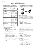
Page 3: ...NTIFIED IN THIS MANUAL FOLLOW THESE PROCEDURES WHENEVER CRITICAL COMPONENTS ARE REPLACED OR IMPROPER OPERATION IS SUS PECTED After correcting the original service problem perform the fol lowing safety checks before releasing the set to the customer 1 Check the area of your repair for unsoldered or poorly sol dered connections Check the entire board surface for solder splashes and bridges 2 Check t...

Page 4: ...val 2 4 3 SAFETY RELATED ADJUSTMENT 3 1 4 ADJUSTMENTS 4 1 5 DIAGRAMS 5 1 Block Diagrams 5 1 5 2 Circuit Boards Location 5 5 5 3 Schematic Diagrams and Printed Wiring Boards 5 6 1 Schematic Diagram of D Board 5 7 2 Schematic Diagram of H Board 5 18 3 Schematic Diagram of A Board 5 19 5 4 Semiconductors 5 22 6 EXPLODED VIEWS 6 1 Chassis 6 1 6 2 Picture Tube 6 2 6 3 Packing Materials 6 3 7 ELECTRICAL...

Page 5: ...esult in a scratched picture tube Clean the cabinet panel and controls with a soft cloth lightly moistened with a mild detergent solution Do not use any type of abrasive pad scouring powder or solvent such as alcohol or benzene Transportation When you transport this monitor for repair or shipment use the original carton and packing materials Use of the tilt swivel This monitor can be adjusted with...

Page 6: ...he supplied Windows Monitor Information Disk onto your PC This monitor complies with the VESA DDC Plug Play standard If your PC graphics board complies with DDC select Plug Play Monitor VESA DDC or this monitor s model name as the monitor type in the Control Panel of Windows 95 98 If your PC graphics board has difficulty communicating with this monitor load the Windows Monitor Information Disk and...

Page 7: ...input signal the resolution of the current input signal 9 GB x Using the control button 1 Display the main MENU Press the center of the control button to display the main MENU on your screen 2 Select the menu you want to adjust Highlight the desired menu by moving the control button towards the rear to go up M towards the front to go down m and left or right to move sideways 3 Adjust the menu Move...

Page 8: ...red in memory for all input signals 1 Press the center of the control button The main MENU appears on the screen 2 Move the control button to highlight CONV and press the center of the control button again The CONVERGENCE menu appears on the screen 3 First move the control button m M to select for horizontal adjustment or for vertical adjustment Then move the control button to adjust the convergen...

Page 9: ...ion when CONTROL LOCK is set to ON RETURN TO MA I N MENU RECOMMENDED RESOLUT I ON F L I CKER TH I N HOR I ZONTAL L I NE D I STORTED SHAPE OUT OF FOCUS D I SCOLORAT I ON HELP SET RESOLUT I ON TO 1 0 2 4X7 6 8 AT 8 5Hz US I NG PC CURRENT SETT I NG I S 1 2 8 0X1 0 2 4 AT 7 5Hz RECOMMENDED RESOLUT I ON SET REFRESH RATE TO 7 5Hz OR 8 5Hz US I NG PC CURRENT SETT I NG I S 6 0Hz F L I CKER RESET 13 GB Tec...

Page 10: ... a magnetic shield near the monitor Try plugging the monitor into a different AC outlet preferably on a different circuit Try turning the monitor 90 to the left or right xProblems caused by the connected computer or other equipment Check your graphics board manual for the proper monitor setting Confirm that the graphics mode VESA Macintosh 16 Color etc and the frequency of the input signal are sup...

Page 11: ...appear white red green blue the monitor is working properly Reconnect the video input cable and check the condition of your computer If the color bars do not appear there is a potential monitor failure Inform your authorized Sony dealer of the monitor s condition If the 1 power indicator is flashing orange Press the 1 power button twice to turn the monitor off and then on If the 1 power indicator ...

Page 12: ...BVTT 3 x 8 5 Three screws BVTT 3 x 8 1 Two screws BVTP 4 x 16 Push screwdriver into opening and remove two claws 6 Release from four claws after slide EMI shield to direction of arrows Claw Claw 2 Two claws Bezel assembly Bezel assembly Cabinet Cabinet 7 EMI shield 3 Cabinet 2 1 ...

Page 13: ... 12 7 Four screws Washer head P3 x 8 2 Cable stopper 5 A board 8 D board 3 Cable cover 4 Cable holder 1 2 A board D board 3 Note The electric potential of heat sink of IC401 is not GND So please do not touch it absolutely to the base chassis and etc which make an ultimate cause of the bad move ment or break 2 2 ...

Page 14: ...4 x 8 Connector 7 pin 6 Four screws Tapping screw 5 11 Deflection yoke 10 Neck assembly 8 Degaussing coil assembly 2 A board 9 Two extention springs 1 Anode cap 12 Two degaussing coil holders 13 Two degaussing coil holders 7 Picture tube Bezel assembly Cushion 8 pin 2 pin CN2 CN601 GND CN303 2 3 ...

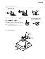
Page 15: ... rubber hardly not to damege inside of anode caps A material fitting called as shatter hook terminal is built in the rubber 3 Don t turn the foot of rubber over hardly The shatter hook terminal will stick out or damage the rubber a b Anode Button c REMOVAL OF ANODE CAP NOTE Short circuit the anode of the picture tube and the anode cap to the metal chassis CRT shield or carbon painted on the CRT af...

Page 16: ... 0 3 0 V DC Check Condition Input voltage 120 2V AC Note Use NF power supply or make sure that distortion factor is 3 or less Input signal White cross hatch at 69 0 kHz Beam control CONT max BRT center HV Regulator Circuit Check HV Protector Circuit Check Beam Current Protector Circuit Check Part Replaced D board IC501 C532 C534 C539 C553 C554 C555 C556 C558 C561 R541 R542 R544 R564 R567 R568 RV50...

Page 17: ...n 8Pin 4 Pin 3 702 691 01 Connector Attachment 3 To BUS CONNECTOR 4 Pin 4 Pin Connect the communication cable of the computer to the connector located on the D board on the monitor Run the service software and then follow the instruction Purity magnet position 6 Adjust the DY position and purity and the DY tilt 7 Fasten DY with screw Note Torque 22 2kgcm 2 2 0 2 Nm 8 Adjust each top and bottom pin...

Page 18: ... B B R XCV YCH TLV TLH Purity Mg 4 pole Mg 6 pole Mg XCV YCH H Trap TLH TLV 4 Pole 6 Pole Neck Assy s Zero Position Purity 2 Digital Convergence Convergence Low Mode 1 Adjust the H STAT and V STAT with HSTAT and VSTAT A Horizontal Convergence Adjust each misconvergence point in sequence B Vertical Convergence CBH T L LO 9 5 10 18 2 20 12 6 17 1 19 11 CBH T R LO MBH T R LO APH R LO MBH B R LO CBH B...

Page 19: ...tion Focus adjustment Adjust the focus volume 1 and 2 for the optimum focus Standard HMC VMC 0 1 mm In the center of screen FBT Focus volume 1 V Focus volume 2 H B Vertical Convergence 2 Repeat the procedure of A and B so that the convergence of the entire screen is within the specification CBH T L HI 9 5 10 18 2 20 12 6 17 1 19 11 CBH T R HI MBH T R HI APH R HI MBH B R HI CBH B R HI MBH T L HI AP...

Page 20: ...CPD E200E 4 4 MEMO ...

Page 21: ...BLK R OSD G OSD 13 B SOD SDA SCL V FLB 5 H FLB 5 4 3 9 8 7 IC004 RGB CUT OFF CONT IC003 OSD SPOT KILLER Q001 IC005 G2 CUT OFF CONT B OUT G OUT R OUT B IN G IN R IN 1 3 4 CN313 B GND 1 G GND 1 2 BLUE 1 GREEN 5 R GND 1 6 RED 1 7 GND 8 VD 1 9 HD 1 TO D BOARD CN902 1 4 A TO D BOARD CN902 5 0 C TO D BOARD CN903 B 1 3 2 4 CN309 C BLK INPUT SELECT BP CLP C SYNC 5 VS OUT 6 GND 7 H SYNC 8 SYNC DET 6 5 4 3 ...

Page 22: ...HP600A CN602 CN601 THP600 1 2kV 1 2 3 H DY 1 H DY H DY V DY CN501 CN510 H DY 4 H DY 5 V DY 6 V DY ROTATION CY DY CN701 ROTATION 1 2 3 ROTATION CY1 4 CY1 5 CY2 6 CY2 7 CY3 8 CY3 9 CY4 10 CY4 15 48 47 44 45 17 38 39 46 22 28 20 30 34 35 33 37 36 25 26 54 21 7 8 5 5 7 4 6 24 6 4 I O I O 5 7 6 13 11 3 1 I O 8 1 2 4 5 9 14 2 ROTATION OUT WC AC IN DGC 3 16 18 19 4 32 23 27 26 4 3 29 12 6 4 8 2 6 4 5 2 3...

Page 23: ...noted e earth ground E earth chassis All voltages are in V Readings are taken with a 10 MΩ digital multimeter Readings are taken with a color bar signal input Voltage variations may be noted due to normal production tolerances Can not be measured Circled numbers are waveform references s B bus S B bus The components identified by in this basic schematic diagram have been carefully factory selected...

Page 24: ... 1 PT 0 1 PT 390p CH CHIP 470 16V 1 5 FPRD 22 1W RS 270 1 4W 0 56 1W 0 68 1W 33 1W RS 2 2 1W RS 100 1W RS 10 220p CH CHIP 0 001 B CHIP 2 7k RN CP 2 7k RN CP 2200 10V 0 1 25V B CHIP 470 JW 5 1SS119 15k RN CP 1 0 10P YEL S MICRO 470 25V 470 25V 33 1W RS 18 1W 68p CH CHIP 68p CH CHIP 10k CHIP 0 1 PT 0 01 B CHIP 0 01 B CHIP 330p B CHIP 4 7k RN CP 15k RN CP 15k RN CP 100 1W RS 2 2 1W RS 0 CHIP 0 CHIP 2...

Page 25: ...RD 1k CHIP HZU5 6B2TRF 22 HZU5 6B2TRF RB501V 40 1 2k 0 100 CHIP MA111 MA111 MA111 MA111 HZU5 6B2TRF HZU5 6B2TRF HZU5 6B2TRF CHIP RB441QT HZS5 6NB2 HZS5 6NB2 0 47 B CHIP 0 47 B CHIP 220 16V 0 CHIP 0 CHIP 0 CHIP 100 CHIP MA111 0 01 B CHIP 2 2k CHIP 2 2k CHIP 8P WHT S MICRO MA111 HZS5 1N MA111 MA111 MA111 1SS119 MA111 1k CHIP 100 CHIP 100 CHIP 100 CHIP 100 CHIP 220 CHIP MA111 4 7k CHIP 4 7k CHIP 0 01...

Page 26: ... HDT 0 0022 100V PT 220k RN ERA34 10TP1 56k RN 62k RN HZT33 02 HZS10N 100 FPRD 4 7 100 25V HT 10 4 7 250V 33 200V 10 50V 4 7 100 16V HSS82 0 1 PT 47k RN CP 47k RN CP 100 10k 33 200V 56 FPRD 33 3W RS ERB91 02TP1 68 1 2W FPRD 4 7 250V 47k 1SS119 22k CHIP 1 15k CHIP 220k 1k HZS5 6NB2 47k 22k CHIP 10K 600MW 1000 25V HT 220 HT 2 2k CHIP 10k CHIP 1000 25V HT 1 5 RN 12k RN CP 12k RN CP 5 6k RN CP ERA34 1...

Page 27: ...RN HV 0 033 200V 330p 2kV B 33 RN CP 22 RN CP MTZJ 18 0 1 PT 1SS119 220 HT 2SC3311A OVP OCP HZS12N EGP10DPKG23 EGP10DPKG23 470 16V 470 16V 3300 16V 2200 16V HT 2200 25V HT 220 25V HT 100 100V 100k 47 200V 47k 2W 2 2k 1 2W FPRD 0 0022 B CHIP 47k 1 2W 100p 500V 2 2k CHIP 110k CHIP 1 FPRD 100 CHIP FMN G12S BA05T 5V REG 220 10V HT 1000 25V 1SS119 0 47 FPRD 0 0047 250V 0 0047 250V BA00AST V5 HEATER OUT...

Page 28: ...5 15 5 16 D Schematic diagram Ò Ò Ò Ò Ò d board D BOARD d CONVERGENCE CONTROL DEDFLECTION CPU POWER SUPPLY 1 2 3 4 5 6 7 A B C D E ...

Page 29: ...19 D 4 D520 C 6 D521 C 6 D522 E 1 D523 E 1 D524 D 5 D525 D 5 D527 C 5 D601 B 6 D602 C 7 D603 B 3 D604 A 3 D605 A 3 D606 A 4 D607 A 4 D608 A 4 D609 A 3 D610 A 4 D611 C 5 D612 B 5 D613 C 5 D614 B 4 D615 B 4 D616 B 4 D617 B 5 D618 C 4 D619 B 4 D620 A 4 D621 C 5 D622 B 4 Refer to Terminal name of semiconductors in silk screen printed circuit see page 5 6 D704 B 1 D901 E 2 3 D902 D 1 3 D903 C 2 D904 E ...

Page 30: ...P 10 250V 0 1 25V B CHIP HSS82 0 1 100V CHIP HSS82 100 1 2W RC 100 1 2W RC 10k 1 2W RC 22M RN 1SS119 0 001 B CHIP 0 1 25V B CHIP 0 1 25V B CHIP 0 1 25V B CHIP 0 1 25V B CHIP 0 1 25V B CHIP 0 1 25V B CHIP 9P WHT S MICRO 1SS119 1SS119 1SS119 1SS119 1SS119 1PS226 115 PROT 1PS226 115 PROT 1PS226 115 PROT 100 CHIP 10k CHIP 10k CHIP 10k CHIP 100 CHIP 100 CHIP 4 7k CHIP 4 7k CHIP 220 CHIP 1k CHIP 9P WHT ...

Page 31: ...TION IC IC001 A 2 IC002 A 3 IC003 A 1 IC004 B 3 IC005 B 3 IC006 B 1 TRANSISTOR Q001 B 3 Q006 B 1 1 DIODE D001 B 3 Refer to Terminal name of semiconductors in silk screen printed circuit see page 5 6 D002 B 1 D003 B 1 D004 B 1 D005 C 3 D007 C 2 D008 C 2 D014 B 3 D015 B 1 D104 A 3 D105 A 2 D106 A 2 D111 B 1 6 D204 A 3 D205 A 3 D206 A 3 D211 B 1 6 D304 A 3 D305 A 3 D306 A 3 D311 B 2 6 1 2 3 A B C ...

Page 32: ...OP PST9143NL 1234 SN74HC02ANSR 1 n 5 pin CHIP STK391 110 1 TOP VIEW n 14 pin SOP TDA8177 MARKING SIDE VIEW 12 n TEA1504 N2 7 1 TL1431CZ 1 TOP VIEW n 14 pin DIP UPC574J DTA114EKA T146 DTC114EK DTC114EKA T146 2SA1037AK T146 QR 2SA1037AK T146 R 2SC1623 L5L6 2SC2412K T 146 QR 1 TOP VIEW n 24 pin DIP DTC143ESA DTC143TSA E B C IRFU110 IRFU110A 2SK2843LBS2SONY 2SK3155 01 B E C 2SA1175 HFE 2SA1309A QRSTA ...

Page 33: ...ODE FMC 26UA FMN G12S FMQ G2FS CATHODE ANODE HZS10NB2 HZS12NB2 HZS4 7NB2 HZS5 6NB2 MTZJ T 77 18 RB4410QT 77 RD10ES B2 RD12ES B2 RD18ES B2 RD5 1ES B2 RD5 6ES B2 1SR139 400 1SS119 25 1 2 1 2 HZU5 6B2TRF MA111 CATHODE ANODE CATHODE ANODE 1 ANODE RED 2 CATHODE 3 ANODE GRN 1 2 3 TLP621D4 RBV501F 40 1 2 3 4 1 2 3 4 UF4007G23 CATHODE ANODE 1PS226 115 CATHODE ANODE SPR 325MVW 1 2 3 2 1 3 ...

Page 34: ... 7 685 646 79 Screw washer head P3X8 7 685 663 71 BVTP 4X16 REF NO PART NO DESCRIPTION REMARK REF NO PART NO DESCRIPTION REMARK SECTION 6 EXPLODED VIEWS The components identified by mark are critical for safety Replace only with part number specified NOTE 6 1 1 2 3 4 5 6 7 8 9 10 1 A 1294 806 A A BOARD COMPLETE 2 4 070 679 02 COVER CABLE 3 4 045 131 01 STOPPER CABLE 4 4 072 384 01 CABINET 5 4 072 ...

Page 35: ... 665 02 BUTTON MENU 56 8 738 550 61 ITC ASSY 17TKB R1 57 60 57 8 738 550 00 PICTURE TUBE 17TKB NORTH 58 8 451 435 12 DEFLECTION YOKE Y17TKJ M 59 1 452 923 41 NECK ASSEMBLY NA 2915 60 2 162 100 21 SPACER DY 61 4 045 123 01 HOLDER DEGAUSSING COIL 62 3 704 372 01 HOLDER HV CABLE 63 4 047 316 01 SPRING EXTENSION 64 4 369 319 00 BAND COIL 65 1 419 255 12 COIL DEGAUSSING 66 4 365 808 01 SCREW 5 TAPPING ...

Page 36: ...ified 6 3 101 102 103 104 107 108 105 106 106 109 101 1 772 398 11 DISK INFORMATION FOR WINDOWS 102 1 765 719 31 CORD SET POWER 103 1 785 512 31 D SUB CONNECTOR 15P CHANGER 104 3 867 657 11 MANUAL INSTRUCTION 105 4 071 985 01 INDIVIDUAL CARTON 106 4 070 062 01 CUSHION UPPER ASSY 107 4 041 927 31 BAG POLYETHYLENE 108 4 070 063 02 CUSHION LOWER ASSY 109 3 701 625 00 BAG POLYETHYLENE ACCESSORY ...

Page 37: ...0 2KV C036 1 104 503 12 CERAMIC CHIP 0 1MF 10 100V C042 1 163 009 11 CERAMIC CHIP 0 001MF 10 50V C044 1 163 251 11 CERAMIC CHIP 100PF 5 50V C046 1 163 021 91 CERAMIC CHIP 0 01MF 10 50V C047 1 104 664 11 ELECT 47MF 20 25V C049 1 164 004 11 CERAMIC CHIP 0 1MF 10 25V C050 1 164 004 11 CERAMIC CHIP 0 1MF 10 25V C053 1 164 004 11 CERAMIC CHIP 0 1MF 10 25V C054 1 137 528 11 MYLAR 0 1MF 10 250V C055 1 10...

Page 38: ...16 296 91 SHORT 0 JR018 1 216 295 91 SHORT 0 JR019 1 216 296 91 SHORT 0 JR020 1 216 296 91 SHORT 0 JR021 1 216 296 91 SHORT 0 COIL L002 1 412 911 11 FERRITE L003 1 408 397 00 INDUCTOR 1UH L005 1 412 529 11 INDUCTOR 22UH L007 1 410 482 31 INDUCTOR 100UH L009 1 216 295 91 SHORT 0 L010 1 412 911 11 FERRITE L102 1 412 052 21 INDUCTOR CHIP 1UH L103 1 414 137 31 INDUCTOR 0 22UH L105 1 410 750 41 INDUCTO...

Page 39: ... 216 113 00 RES CHIP 470K 5 1 10W R330 1 216 022 00 RES CHIP 75 5 1 10W R351 1 202 549 00 SOLID 100 20 1 2W R361 1 215 394 00 METAL 75 1 1 4W SPARK GAP SG001 1 519 422 11GAP SPARK SG002 1 517 499 21GAP SPARK SG101 1 517 499 21GAP SPARK SG201 1 517 499 21GAP SPARK SG301 1 517 499 21GAP SPARK A 1346 877 A D BOARD COMPLETE 4 382 854 01 SCREW M3X8 P SW IC401 IC503 IC602 IC605 IC607 IC608 Q503 Q510 Q52...

Page 40: ... 0047MF 20 250V C608 1 104 653 91 ELECT 220MF 20 16V C610 1 107 852 11 ELECT BLOCK 330MF 20 400V C611 1 163 007 11 CERAMIC CHIP 680PF 10 50V C612 1 106 379 12 MYLAR 0 033MF 10 200V C613 1 162 115 00 CERAMIC 330PF 10 2KV C614 1 163 021 91 CERAMIC CHIP 0 01MF 10 50V C615 1 163 037 11 CERAMIC CHIP 0 022MF 10 50V C616 1 107 907 11 ELECT 22MF 20 25V C617 1 107 907 11 ELECT 22MF 20 25V C618 1 130 495 00...

Page 41: ...G2FS D507 8 719 109 85 ZENER DIODE RD5 1ESB2 D509 8 719 110 17 ZENER DIODE RD10ESB2 D510 8 719 018 82 DIODE RGP02 20EL 6394 D511 8 719 109 89 ZENER DIODE RD5 6ESB2 D512 8 719 911 19 DIODE 1SS119 25 D513 8 719 052 90 DIODE D1NL40 TA2 D514 8 719 970 83 DIODE HSS82 D515 8 719 018 82 DIODE RGP02 20EL 6394 D516 8 719 052 86 DIODE D2L40 TA D517 8 759 157 40 IC uPC574J D518 8 719 110 17 ZENER DIODE RD10E...

Page 42: ...03 8 759 822 38 IC LA6510 IC901 8 759 596 69 IC CXD9528S IC902 8 759 594 40 IC CXA8071CP IC904 8 759 352 91 IC PST9143NL IC905 8 759 527 76 IC M24C08 MN6T CHIP CONDUCTOR JR001 1 216 296 91 SHORT 0 JR003 1 216 295 91 SHORT 0 JR004 1 216 295 91 SHORT 0 JR006 1 216 295 91 SHORT 0 JR007 1 216 295 91 SHORT 0 JR008 1 216 296 91 SHORT 0 JR009 1 216 295 91 SHORT 0 JR010 1 216 296 91 SHORT 0 JR011 1 216 29...

Page 43: ...1 247 863 91 CARBON 22K 5 1 4W R510 1 215 437 00 METAL 4 7K 1 1 4W R511 1 249 381 11 CARBON 1 5 1 4W F R512 1 249 389 11 CARBON 4 7 5 1 4W R513 1 215 888 00 METAL OXIDE 220 5 2W F R514 1 216 081 00 RES CHIP 22K 5 1 10W R515 1 249 417 11 CARBON 1K 5 1 4W F R516 1 214 844 81 METAL 150 1 1 2W R517 1 216 393 00 METAL OXIDE 2 2 5 3W F R518 1 216 393 00 METAL OXIDE 2 2 5 3W F R519 1 215 463 00 METAL 56K...

Page 44: ...10W R629 1 249 441 11 CARBON 100K 5 1 4W R630 1 211 874 71 FUSIBLE MELF 0 12 10 1 2W R631 1 211 874 71 FUSIBLE MELF 0 12 10 1 2W R633 1 249 429 11 CARBON 10K 5 1 4W R634 1 211 874 71 FUSIBLE MELF 0 12 10 1 2W R635 1 215 925 11 METAL OXIDE 22K 5 3W F R636 1 260 119 11 CARBON 47K 5 1 2W R637 1 215 902 11 METAL OXIDE 47K 5 2W F R638 1 211 874 71 FUSIBLE MELF 0 12 10 1 2W R639 1 211 874 71 FUSIBLE MEL...

Page 45: ...ON 470 5 1 4W R951 1 216 025 91 RES CHIP 100 5 1 10W R953 1 216 073 00 RES CHIP 10K 5 1 10W R954 1 216 073 00 RES CHIP 10K 5 1 10W R957 1 216 017 91 RES CHIP 47 5 1 10W R958 1 216 017 91 RES CHIP 47 5 1 10W VARIABLE RESISTOR RV501 1 241 767 21RES ADJ CERMET 100K HV ADJ 3 710 578 01COVER VOLUME 6 MOLD RV501 RELAY RY500 1 515 669 21RELAY RY601 1 755 279 11RELAY SWITCH S602 1 771 757 11 SWITCH AC POW...

Page 46: ...0 METAL 3 3K 1 1 4W R805 1 247 807 31 CARBON 100 5 1 4W R806 1 247 807 31 CARBON 100 5 1 4W R807 1 249 411 11 CARBON 330 5 1 4W R808 1 249 413 11 CARBON 470 5 1 4W SWITCH S801 1 771 734 11 SWITCH TACTILE BRIGHT MENU CONT CPD E200E 9 978 669 01 2000AL24126 1 7 10 56 Sony Corporation Computer Display Division Company Computer Display Div 9 978 669 01 English 2000AL24126 1 Printed in Japan 2000 1 ...

Reviews: