background image

— 4 —

DSC-P9

TABLE OF CONTENTS

1.

SERVICE NOTE

························································ 1-1

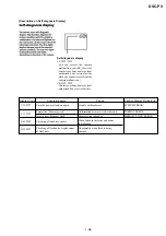
Self-diagnosis Display ····················································· 1-3

2.

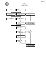
DISASSEMBLY

2-1.

BT Lid ············································································· 2-2

2-2.

Cabinet (Front) Assembly ··············································· 2-2

2-3.

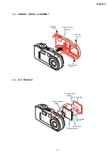
Cabinet (Rear) Assembly ················································· 2-3

2-4.

LCD Module ···································································· 2-3

2-5.

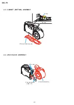
Cabinet (Bottom) Assembly ············································ 2-4

2-6.

Lens Block Assembly ······················································ 2-4
Service Position (SY-77 Board: Side A) ·························· 2-5

2-7.

Control Switch Block ······················································ 2-5

2-8.

SY-77 Board ···································································· 2-6

2-9.

Memory Stick Connector ················································ 2-6

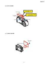
2-10. ST-70 Board ····································································· 2-7
2-11. SW-368 Board ································································· 2-7
2-12. JK-227 Board ·································································· 2-8

Service Position (SY-77 Board: Side B) ·························· 2-8

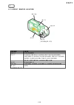
2-13. Circuit Boards Location ·················································· 2-9

3.

BLOCK DIAGRAMS

3-1.

Overall Block Diagram ··················································· 3-1

3-8.

Power Block Diagram 1 ················································ 3-15

3-9.

Power Block Diagram 2 ················································ 3-17

4.

PRINTED WIRING BOARDS AND
SCHEMATIC DIAGRAMS

4-1.

Frame Schematic Diagrams ············································· 4-1
Frame Schematic Diagram (1/2) ····································· 4-1
Frame Schematic Diagram (2/2) ····································· 4-3

4-2.

Schematic Diagrams ························································ 4-5

CD-397 (CCD IMAGER) ··············································· 4-7
SW-368 (1/2) (CONTROL SWITCH) ·························· 4-29
SW-368 (2/2)
(LCD DRIVE, TIMING GENERATOR) ····················· 4-31
ST-70 (FLASH DRIVE) ··············································· 4-35

4-3.

Printed Wiring Boards ··················································· 4-39
CD-397 ·········································································· 4-41
SW-368 ·········································································· 4-47
ST-70 ············································································· 4-51

4-4.

Waveforms ····································································· 4-54

4-5.

Parts Location ································································ 4-57

5.

ADJUSTMENTS

Before Starting Adjustment ······················································· 5-1
1-1.

Adjusting Items when Replacing
Main Parts and Boards ···················································· 5-2

5-1.

Camera Section Adjustments ··········································· 5-3

1-1.

Preparations Before Adjustment ······································ 5-3

1-1-1. List of Service Tools ························································ 5-3
1-1-2. Preparations ····································································· 5-4
1-1-3. Discharging of the Flashlight Power Supply ··················· 5-4
1-1-4. Precautions ······································································ 5-6
1.

Setting the Switch ···························································· 5-6

2.

Order of Adjustments ······················································ 5-6

3.

Subjects ··········································································· 5-6

4.

Preparing the Flash Adjustment Box ······························· 5-7

1-2.

Initialization of A, B, D, E, F, 7, 9 Page Data ················· 5-8

1-2-1. Initialization of A, D Page Data ······································ 5-8
1.

Initializing A, D Page Data ·············································· 5-8

2.

Modification of A, D Page Data ······································ 5-8

3.

A Page Table ···································································· 5-8

4.

D Page Table ···································································· 5-8

Section

Title

Page

Section

Title

Page

1-2-2. Initialization of B, E, F, 7, 9 Page Data ··························· 5-9
1.

Initializing B, E, F, 7, 9 Page Data ·································· 5-9

2.

Modification of B, E, F, 7, 9 Page Data. ·························· 5-9

3.

B Page Table ···································································· 5-9

4.

E Page Table ···································································· 5-9

5.

F Page Table ·································································· 5-10

6.

7 Page Table ··································································· 5-12

7.

9 Page Table ··································································· 5-12

1-3.

Video System Adjustments ············································ 5-13

1.

Video Sync Level Adjustment ······································· 5-13

2.

Video Burst Level Check ··············································· 5-13

1-4.

Camera System Adjustments ········································· 5-14
Data Setting During Camera System Adjustments ········ 5-14
Picture Frame Setting ···················································· 5-15
Check on the Oscilloscope ············································ 5-15

1.

Flange Back Adjustment
(Using the minipattern box) ·········································· 5-16

2.

Flange Back Adjustment
(Using the flange back adjustment chart) ······················ 5-17

3.

Flange Back Check ························································ 5-17

4.

F No. Compensation ······················································ 5-18

5.

Mechanical Shutter Adjustment ···································· 5-18

6.

Light Value Adjustment ················································· 5-19

7.

Mixed Color Cancel Adjustment ··································· 5-19

8.

Auto White Balance 3200K Standard Data Input 1 ······ 5-20

9.

Auto White Balance 3200K Standard Data Input 2 ······ 5-21

10.

Auto White Balance 3200K Standard Data Input 3 ······ 5-21

11.

Auto White Balance 3200K Check ······························· 5-22

12.

Auto White Balance 5800K Standard Data Input 1 ······ 5-23

13.

Auto White Balance 5800K Standard Data Input 2 ······ 5-24

14.

Auto White Balance 5800K Standard Data Input 3 ······ 5-24

15.

Auto White Balance 5800K Check ······························· 5-25

16.

CCD Linearity Check ···················································· 5-26

17.

Color Reproduction Adjustment ···································· 5-27

18.

CCD White Defect Compensation ································ 5-28

19.

CCD Black Defect Compensation ································· 5-29

20.

Strobe White Balance Adjustment ································· 5-30

21.

AF Illumination Check ·················································· 5-32

1-5.

LCD System Adjustments ············································· 5-33

1.

LCD Initial Data Input ·················································· 5-34

2.

VCO Adjustment (SW-368 Board) ································ 5-34

3.

Black Limit Adjustment (SW-368 Board) ····················· 5-35

4.

Bright Adjustment (SW-368 Board) ······························ 5-35

5.

Contrast Adjustment (SW-368 Board) ·························· 5-36

6.

VG Center Adjustment (SW-368 Board) ······················· 5-36

7.

PSIG Gray Adjustment (SW-368 Board) ······················ 5-37

8.

V-COM Adjustment (SW-368 Board) ··························· 5-37

9.

White Balance Adjustment (SW-368 Board) ················ 5-38

5-2.

Service Mode ································································· 5-39

2-1.

Adjusting Remote Commander ····································· 5-39

1.

Used the Adjusting Remote Commander ······················ 5-39

2.

Precautions upon Using the Adjusting
Remote Commander ······················································ 5-39

2-2.

Data Process ·································································· 5-40

2-3.

Service Mode ································································· 5-41

1.

Setting the Test Mode ···················································· 5-41

2.

Bit Value Discrimination ··············································· 5-41

3.

Mode Dial Check (1) ····················································· 5-41

4.

Mode Dial Check (2) ····················································· 5-41

5.

Switch Check (1) ··························································· 5-41

6.

Switch Check (2) ··························································· 5-42

7.

LED Check ···································································· 5-42

8.

Self Diagnosis Code ······················································ 5-42

Summary of Contents for Cyber-shot DSC-P9

Page 1: ...m printed wiring board and electrical parts list of the JK 226 JK 227 SY 77 boards are not shown The following pages are not shown SY 77 board Schematic diagram Pages 4 9 to 4 28 Printed wiring board Pages 4 43 to 4 46 Electrical parts list Pages 6 9 to 6 13 JK 226 JK 227 boards Schematic diagram Pages 4 33 to 4 34 Printed wiring board Pages 4 49 to 4 50 Electrical parts list Pages 6 6 The above d...

Page 2: ...nches W H D protruding parts not included Mass Approx 180 g 6 oz adaptor only NP FC10 battery pack Used battery Lithium ion battery Maximum voltage DC 4 2 V Nominal voltage DC 3 6 V Capacity 2 4 Wh 675 mAh Accessories A V connecting cable 1 NP FC10 battery pack 1 AC LS1A AC power adaptor 1 Power cord mains lead 1 USB cable 1 Wrist strap 1 Memory Stick 16MB 1 CD ROM USB driver SPVD 008 1 Operating ...

Page 3: ... melts at a temperature about 40 C higher than ordinary solder Ordinary soldering irons can be used but the iron tip has to be applied to the solder joint for a slightly longer time Soldering irons using a temperature regulator should be set to about 350 C Caution The printed pattern copper foil may peel away if the heated tip is applied for too long so be careful Strong viscosity Unleaded solder ...

Page 4: ...5 9 4 E Page Table 5 9 5 F Page Table 5 10 6 7 Page Table 5 12 7 9 Page Table 5 12 1 3 Video System Adjustments 5 13 1 Video Sync Level Adjustment 5 13 2 Video Burst Level Check 5 13 1 4 Camera System Adjustments 5 14 Data Setting During Camera System Adjustments 5 14 Picture Frame Setting 5 15 Check on the Oscilloscope 5 15 1 Flange Back Adjustment Using the minipattern box 5 16 2 Flange Back Adj...

Page 5: ... Views 6 1 6 1 1 Cabinet Front Section 6 1 6 1 2 Cabinet Rear Assembly 6 2 6 1 3 Lens Block and LCD Section 6 3 6 1 4 Battery Holder Assembly 6 4 6 2 Electrical Parts List 6 5 Section Title Page The color reproduction frame is shown on page 113 ...

Page 6: ...resistor of 1 kΩ 1 W 1 215 869 11 Wrap insulating tape fully around the leads of the resistor to prevent electrical shock 1 kΩ 1 W Wrap insulating tape Discharging the Capacitor Short circuit between the positive and the negative terminals of charged capacitor with the short jig about 10 seconds NOTE FOR REPAIR Make sure that the flat cable and flexible board are not cracked of bent at the termina...

Page 7: ...e power off 2 Replace the video lens with a new one turn the power on and perform the Flange Back Adjustment Thus new position data will be written 3 After the Flange BackAdjustment return the bit value of Bit0 on Page 9 Address 17 to 1 using the adjusting remote commander When Replacing the SY 77 Board 1 Replace the SY 77 board with a new one set the mode dial to PLAY turn the power on and set th...

Page 8: ...orized Sony service facility Display Code C 32 ss C 13 ss Countermeasure Turn the power off and on again Format the Memory stick Insert a new Memory Stick Cause Trouble with hardware Unformatted memory stick is inserted Memory stick is broken Caution Display During Error SYSTEM ERROR FORMAT ERROR MEMORY STICK ERROR E 61 ss E 91 ss Checking of lens drive circuit When failed in the focus and zoom in...

Page 9: ...LID Page 2 2 2 7 CONTROL SWITCH BLOCK Page 2 5 2 5 CABINET BOTTOM ASSEMBLY Page 2 4 2 4 LCD MODULE Page 2 3 DSC P9 2 10 ST 70 BOARD Page 2 7 2 11 SW 368 BOARD Page 2 7 2 8 SY 77 BOARD Page 2 6 2 6 LENS BLOCK ASSEMBLY Page 2 4 2 9 MEMORY STICK CONNECTOR Page 2 6 SERVICE POSITION SY 77 BOARD side A Page 2 5 2 12 JK 227 BOARD Page 2 8 SERVICE POSITION SY 77 BOARD side B Page 2 8 ...

Page 10: ...BLY 2 1 BT LID Note Follow the disassembly procedure in the numerical order given 4 BT lid 2 Screw 1 7 3 3 Two claws 1 Open the BT lid 3 Two screws M1 7 6 Screw M1 7 2 Screw M1 7 1 Screw M1 7 5 Cabinet front assembly 4 7 Center cabinet ...

Page 11: ... CABINET REAR ASSEMBLY 2 4 LCD MODULE 3 Two screws M1 7 1 Screw M1 7 2 Screw M1 7 5 Cabinet rear assembly 4 3 Two screws M1 7 5 Back light unit 6 LCD module 4 Four claws 1 Flexible board CN102 2 Flexible board CN101 ...

Page 12: ...2 4 DSC P9 2 6 LENS BLOCK ASSEMBLY 2 5 CABINET BOTTOM ASSEMBLY 2 Cabinet bottom assembly 1 Claw Rear side 1 Two flexible board CN001 301 3 Lens block assembly 2 Two claws ...

Page 13: ...der 1 1 18 18 CPC 9 jig J 6082 393 C Regulated power supply 6 0 to 7 2 Vdc AC power adaptor AC IN SY 77 board LCD module Back light unit Lens block assembly Color monitor Base Note 1 Don t use the 12 pin flexible board of CPC 9 jig It causes damage to the unit Note 2 The old CPC 9 jig Parts code J 6082 393 B cannot be used because it cannot operate the adjustment remote commander ...

Page 14: ...BOARD 2 9 MEMORY STICK CONNECTOR 2 Claw 3 Memory stick connector 1 Two screws M1 7 4 5 Claw 7 SY 77 board 1 Connector CN351 3 Three flexible boards CN001 301 702 6 Flexible board CN701 2 Flexible board CN703 4 Screw M1 7 4 ...

Page 15: ... 2 11 SW 368 BOARD 2 SW 368 board 1 Two screws M1 7 4 3 ST 70 board 1 Connector CN351 2 Claw BT main frame Note High voltage cautions See page 1 1 Note When installing ST 70 board the claw is put into the bottom the BT main frame ...

Page 16: ...368 board ST 70 board Memory stick connector Lens block assembly Color monitor LCD module Back light unit Note 1 Don t use the 12 pin flexible board of CPC 9 jig It causes damage to the unit Note 2 The old CPC 9 jig Parts code J 6082 393 B cannot be used because it cannot operate the adjustment remote commander 2 12 JK 227 BOARD 7 JK 227 board including JK 226 1 Screw M1 7 4 5 Screw M1 7 4 DD shee...

Page 17: ...RA MODULE CAMERA DSP VIDEO MEMORY LENS DRIVE SH DSP FLASH MEMORY FRONT CONTROL AUDIO CLOCK GENERATOR FLASH CONTROL DC DC CONVERTER CAMERA PROCESS ST 70 FLASH DRIVE SW 368 CONTROL SWITCH LCD DRIVE TIMING GENERATOR JK 227 JACK including JK 226 SW 368 ST 70 CD 397 SY 77 JK 227 including JK 226 ...

Page 18: ...DSC P9 COVER COVER Link Link 3 BLOCK DIAGRAMS POWER BLOCK DIAGRAM 1 OVERALL BLOCK DIAGRAM POWER BLOCK DIAGRAM 2 POWER BLOCK DIAGRAM 1 OVERALL BLOCK DIAGRAM POWER BLOCK DIAGRAM 2 ...

Page 19: ...C102 LCD TIMING GENERATOR 2 2 CV OUT V OUT AU OUT COLOR LCD MONITOR D901 BACK LIGHT PANEL UNIT LCD SO XLCD SCK LCD SO XLCD SCK J002 SW 368 BOARD 1 2 JK 226 BOARD 2 2 JK 227 BOARD 2 2 IC403 INITIAL RESET BACK UP VCC 7 10 FR 5V EVER 3 0V FUNCTION SWITCH 4 10 VR VG VB VAMP ON BEEP BEEP ON RESET X501 27MHz CAM 3 2V CAM 7 5V A 4 9V A 2 9V D 1 5V D 2 9V PANEL 2 9V BL VO FR 5V A V OUT MONO LCD901 05 ZOOM...

Page 20: ...1 D 1 5V EVER 3 0V PWR LED VCC HI UNREG CPC FOR CHECK D 2 9V D 2 9V POWER 1 D 2 9V S ST 70 BOARD JK 227 BOARD JK 226 BOARD IC403 INITIAL RESET BACK UP VCC 7 10 IC404 FRONT CONTROLLER 7 10 CN351 VL 3V ST UNREG DC IN J001 ACV UNREG GND BATT XEXT ACV UNREG1 BATT XEXT Q017 018 INIT CHARGE FAST CHARGE BATT SIG DD CON SENS BATT XEXT BT901 BATTERY TERMINAL BATT UNREG1 BATT SIG BATT GND 48 68 47 8 42 43 F...

Page 21: ...15V CAM 7 5V 24 FB502 M 5V FB101 FB151 L153 FB153 L154 L101 FB152 CCD IMAGER IC101 CD 397 BOARD POWER 1 PAGE 3 16 CAM 15V CAM 7 5V A 4 9V CAM 3 2V M 5V D 2 9V D 1 5V A 2 9V CAM 15V CAM 7 5V A 4 9V CAM 3 2V M 5V M 5V D 2 9V D 2 9V D 1 5V A 2 9V A MEMORY STICK CN702 2 6 Q701 VCC Q152 153 32 33 CN701 L303 L302 L301 L101 L203 14 XP OFF 13 5V REG Q002 003 L101 L104 D002 FLASH CHG D004 TALLY D003 AE LOC...

Page 22: ...L BL_THH NC BL_H S004 HSY LANC_OUT CPC_IN N C HI_UNREG PANEL_COM N C N C VG LANC_IN N C N C REG_GND N C N C XPB_ON XSHTR_SW XAE_LOCK_SW XMOVIE GND XPWR_ON PWR_LED_VCC MODE_DIAL NC NC D_2 9V NC XPWR_LED XSET_UP MIC_SIG REG_GND PANEL_R REG_GND PANEL_COM KEY_AD0 PANEL_HDD BL_VO A_4 9V PANEL_G XCHARGE_LED CAM_15V PANEL_B REG_GND PANEL_VG EVER_3 0V LCD_SO PANEL_2 9V XLCD_SCK AE_LOCK_LED PANEL_2 9V REG_...

Page 23: ...8 FLEXIBLE BOARD F_RST_SENS SHUTTER F_RST_GND Z_RST_VCC FOCUS_B Z_POSI_OUT SUTTEER ZOOM_A IRIS_S FOCUS_A ZOOM_B FOCUS_A IRIS_S TEMP_OUT Z_RST_GND SHUTTER Z_POSI_VCC ZOOM_B ZOOM_A SHUTTER Z_POSI_GND TEMP_GND F_RST_VCC FOCUS_B Z_RST_SENS GND GND ACV_UNREG1 ACV_UNREG1 BATT_UNREG1 GND AV_GND ACV_UNREG1 BATT_UNREG1 GND USB_DATA V_OUT ACV_UNREG1 BATT_UNREG1 GND USB_DATA AV_GND ACV_UNREG1 GND BATT SIG BA...

Page 24: ...OG A AUDIO SIGNAL ANALOG A VIDEO AUDIO SIGNAL A VIDEO AUDIO SERVO SIGNAL A SERVO SIGNAL Circled numbers refer to waveforms Measuring conditions voltage and waveform Voltages and waveforms are measured between the measurement points and ground when camera shoots color bar chart of pattern box They are reference values and reference waveforms VOM of DC 10 MΩ input impedance is used Voltage values ch...

Page 25: ...NG GENERATOR CONTROL SWITCH BLOCK ST 70 BOARD FLASH DRIVE CD 397 BOARD CCD IMAGER SW 368 BOARD 1 2 CONTROL SWITCH SW 368 BOARD 2 2 LCD DRIVE TIMING GENERATOR CONTROL SWITCH BLOCK ST 70 BOARD FLASH DRIVE CD 397 BOARD CCD IMAGER COMMON NOTE FOR SCHEMATIC DIAGRAMS WAVEFORMS COMMON NOTE FOR SCHEMATIC DIAGRAMS WAVEFORMS ...

Page 26: ...17 CSUB 18 VL 19 H1 20 H2 XX R109 1 A 8 14 4 9 1 15 18 19 10 2 16 6 25 23 24 22 20 12 11 3 21 7 13 5 17 C E BUFFER 2 IC101 3 SY 77 1 10 CCD IMAGER CCD BLOCK CN001 CCD IMAGER 4 B D 8 6 5 F 7 05 SWITCH PAGE 4 9 XX MARK NO MOUNT CD 397 BOARD SIGNAL PATH VIDEO SIGNAL Y CHROMA REC SELF TIMER AF ILLUMINATOR CCD TEMP SENSOR 4 2 SCHEMATIC DIAGRAMS For Schematic Diagram Refer to page 4 41 for printed wirin...

Page 27: ... CL024 CL029 CL016 CL027 CL026 CL020 CL023 CL019 CL017 CL025 CL015 CL022 CL018 CL021 CL032 CL030 CL031 CL033 HN1A01FU TE85R Q003 HN1C01FU TE85R Q002 UN9213J K8 SO Q004 CL028 XX R004 1 A PANEL_COM PANEL_VG PANEL_HDO PANEL_R PANEL_G PANEL_B XRST_SYS HDO PANEL_V LCD_SO XLCD_SCK XCS_PANEL_TG BL_VO A_4 9V BL_VO BL_VO PANEL_HDO HDO PANEL_V LCD_SO XCS_PANEL_TG XLCD_SCK PANEL_R PANEL_G PANEL_B PANEL_COM P...

Page 28: ...6 GND 7 TST0 8 LED 9 PWM 10 TEST 11 TEST 12 TEST 13 TSTEN 14 XP_OFF 15 RGT 16 HCK1 17 HCK2 18 HST 21 DWN 19 VDD 20 WIDE 22 EN 23 VCK 24 VST 25 XSTBY 26 OSCO 27 OSCI 28 XC SAVE 29 RPD 30 TEST 31 VSS 32 SHA 33 SHB 34 SHG 35 SHR 36 XCLR 37 XCLP 38 PRG 39 SBLK 40 FRP 41 PFRP 42 XSCK 45 SO 44 XCS 43 VDD 46 SI 47 VDO 48 XVD 24P CN102 1 2 3 4 5 6 7 8 9 10 11 12 13 14 15 16 17 18 19 20 21 22 23 24 XLCD_SC...

Page 29: ...EG_GND LND011 REG_GND 1 A P F S 10 5 8 7 6 1 4 9 3 2 11 12 14 15 13 FLASH DRIVE PAGE 4 26 SY 77 9 10 CN351 3 10 7 C 5 D B E 9 6 8 4 2 FLASH DRIVE FL BLOCK ST 70 BOARD 05 LITHIUM BATTERY BACK UP CHARGING CAPACITOR Q001 2SB1073 R TX TRANS DRIVE FLASH UNIT 4 2 SCHEMATIC DIAGRAMS ST 70 PRINTED WIRING BOARD 4 2 SCHEMATIC DIAGRAMS ST 70 PRINTED WIRING BOARD For Schematic Diagram Refer to page 4 51 for p...

Page 30: ... 12 13 14 1 A S005 SET_UP MOVIE PLAY 5 POSITION MODE_DIAL P_AUTO SCN 05 B D CONTROL SWITCH BLOCK 3 E 2 C 4 5 CONTROL SWITCH BLOCK is replaced as a block so that PRINTED WIRING BOARD is omitted S004 SHUTTER 20k R001 D001 POWER GREEN MODE DIAL POWER S003 2nd 1st XPWR_ON NC PWR_LED_VCC XPWR_LED XMOVIE XPB_ON NC XSET_UP GND NC MODE_DIAL D_2 9V XSHTR_SW XAE_LOCK_SW SEE PAGE 4 21 SY 77 7 10 CN704 ...

Page 31: ...ole is omitted Circled numbers refer to waveforms There are a few cases that the part printed on diagram isn t mounted in this model C panel designation THIS NOTE IS COMMON FOR WIRING BOARDS In addition to this the necessary note is printed in each block 2 1 3 2 1 3 2 1 3 3 4 5 2 1 1 2 3 6 5 4 E B C 3 1 5 5 2 4 6 1 2 3 5 4 4 3 1 2 1 2 4 3 3 1 2 4 5 5 3 4 1 2 3 4 2 1 1 2 4 3 4 6 2 5 3 1 1 2 4 3 Chi...

Page 32: ...97 BOARD SW 368 BOARD ST 70 BOARD CD 397 BOARD SW 368 BOARD ST 70 BOARD CIRCUIT BOARDS LOCATION WAVEFORMS COMMON NOTE FOR PRINTED WIRING BOARDS MOUNTED PARTS LOCATION CIRCUIT BOARDS LOCATION WAVEFORMS COMMON NOTE FOR PRINTED WIRING BOARDS MOUNTED PARTS LOCATION ...

Page 33: ...MATIC DIAGRAMS 4 3 PRINTED WIRING BOARDS MOUNTED PARTS LOCATION MOUNTED PARTS LOCATION CD 397 4 41 4 42 CD 397 CCD IMAGER For Printed Wiring Board Uses unleaded solder There are a few cases that the part isn t mounted in this model is printed on this diagram SELF TIMER AF ILLUMINATOR ...

Page 34: ...4 48 SW 368 FRONT CONTROL LCD DRIVE TIMING GENERATOR CONTROL SWITCH For Printed Wiring Board Uses unleaded solder There are a few cases that the part isn t mounted in this model is printed on this diagram See page 4 57 for printed parts location CONTROL D003 AE LOCK GREEN D004 TALLY RED D002 STROBO CHARGE LED DISPLAY MENU ZOOM W T 6 7 5 1 2 3 4 10 8 9 A K K A K K A K K K A K ...

Page 35: ...RING BOARDS MOUNTED PARTS LOCATION MOUNTED PARTS LOCATION 4 51 4 52 ST 70 ST 70 FLASH DRIVE For Printed Wiring Board Uses unleaded solder There are a few cases that the part isn t mounted in this model is printed on this diagram BT001 BATTERY LITHIUM SECONDARY C B E 1 2 4 6 3 5 A A K FLASH UNIT 11 12 11 12 ...

Page 36: ... REC PB 7 8 Vp p 2H 4 IC101 wj REC PB 5 1 Vp p 2H 2H 2H 2H 7 5 6 8 IC101 rh REC PB 340 mVp p IC102 1 REC PB H 3 0 Vp p IC101 rk REC PB H 460 mVp p H IC101 rj REC PB 340 mVp p H 9 q 11 28 MHz IC102 wj REC PB 4 1 Vp p IC102 rk REC PB 3 0 Vp p V SW 368 BOARD SW 368 BOARD SW 368 BOARD SW 368 ...

Page 37: ...01 B 2 L102 C 3 L103 B 3 L104 B 2 Q002 C 2 Q003 C 2 Q004 A 2 Q101 B 4 Q102 B 4 Q103 C 2 Q104 C 3 Q105 A 2 Q106 C 2 Q107 A 2 Q108 A 3 Q109 C 2 R002 C 2 R003 C 2 R005 B 2 R006 C 2 R007 A 2 R008 A 2 R009 A 2 R010 A 4 R011 C 2 R012 B 1 R013 B 1 R014 C 1 R015 C 1 R018 A 2 R104 B 4 R105 B 4 R106 B 3 R107 B 4 R108 B 3 R109 B 3 R110 B 3 SW 368 BOARD R111 B 3 R112 C 3 R113 C 3 R114 B 3 R115 C 4 R116 C 4 R1...

Page 38: ...saved due to defective EEPROM or when the EEPROM cannot be removed or in stalled save the data from the same model of the same destination and download it PC Save the EVR data to a personal computer Download the saved data to a machine Procedure 1 Save the EVR data of the machine in which a board is going to be replaced Download the saved data after a board is replaced Machine after a board is rep...

Page 39: ...368 board SY 77 board Supporting Initialization of A B D Initialization of A D page data z z E F 7 9 page data Initialization of B E F 7 9 page data z z Video Video sync level adj z z z z z Video burst level check z z z Camera Flange back adj z z z z z F No compensation z z z z z Mechanical shutter adj z z z z z Light value adj z z z z z z Mixed color cancel adj z z z z z z Auto white balance stan...

Page 40: ...nnecting the adjusting remote commander For adjusting the LCD block For adjusting the flange back J 9 Back ground paper J 2501 130 A For adjusting the strobe 5 1 CAMERA SECTION ADJUSTMENT 1 1 PREPARATIONS BEFORE ADJUSTMENT 1 1 1 List of Service Tools Oscilloscope Color monitor Vectorscope Regulated power supply Digital voltmeter Note 1 If the micro processor IC in the adjusting remote commander is...

Page 41: ...be turned on After completing adjustments be sure to exit the Forced CAMERA mode power ON Mode Note 4 Exiting the Forced CAMERA mode power ON Mode 1 Select page 0 address 01 and set data 01 2 Select page D address 21 set data 00 and press the PAUSE button of the adjusting remote com mander 3 Select page 0 address 01 and set data 00 1 1 3 Discharging of the Flashlight Power Supply The capacitor whi...

Page 42: ...o 7 2 Vdc CPC 9 jig Note 1 2 J 6082 393 C 18 1 Adjusting remote commander SW 368 BOARD PANEL UNIT Audio Black Video yellow Color monitor Vectorscope Terminated 75 Ω AC IN AC power adaptor JK 226 BOARD JK 227 BOARD DC IN jack A V OUT jack CN351 CN704 CN705 CN001 CN301 CN702 CN703 CN701 CN706 J001 CN002 J002 CN101 CN102 USB jack Must be connected when the Memory Stick is used Must be connected when ...

Page 43: ...ar chart from the pattern box and insert a clear chart in its place Do not perform zoom operations dur ing this time 3 Chart for flange back adjustment Join together a piece of white A0 size paper 1189mm 841 mm and a piece of black paper to make the chart shown in Fig 5 1 8 Note Use a non reflecting and non glazing vellum paper The size must be A0 or larger and the joint between the white and blac...

Page 44: ...00 mm 370 mm woody board C 1 1000 mm 700 mm 1026 mm Depth 1 m 513 mm Depth 50 cm 1026 mm Depth 1 m 513 mm Depth 50 cm 1000 mm 700 mm 1000 mm 700 mm 1030 mm 730 mm 2 Apply black mat paint to one side of woody board A and B 3 Attach background paper J 2501 130 A to woody board C 4 Assemble so that the black sides and the background paper side of woody board A B and C are internal Fig 5 1 10 Fig 5 1 ...

Page 45: ...justing remote commander each time when setting new data to write the data in the non volatile memory 4 Check that the data of adjustment addresses is the initial value If not change the data to the initial value Processing after Completing Modification of A D Page Data Order Page Address Data Procedure 1 2 00 29 2 2 01 29 Press PAUSE button 3 A Page table Note 1 Fixed data 1 Initialized data Refe...

Page 46: ...e different in destination When changing the data copy the data built in the same model Note If copy the data built in the different model the camera may not operate 3 When changing the data press the PAUSE button of the adjusting remote commander each time when setting new data to write the data in the non volatile memory 4 Check that the data of adjustment addresses is the initial value If not c...

Page 47: ...9 00 2A 00 2B 00 2C 00 2D 00 2E 00 2F 00 30 00 31 00 32 00 33 00 34 00 35 00 36 00 37 00 38 00 39 00 3A 00 3B 00 3C 00 3D 00 Address Initial value Remark 3E FF Flange back adj 3F Fixed data 1 Initialized data 40 00 Flange back adj 41 00 42 00 43 00 44 00 45 00 46 00 47 00 48 00 49 00 4A 00 4B 00 4C 00 4D 00 4E 00 4F 00 50 00 51 00 52 00 53 00 54 to 5D Fixed data 1 Initialized data 5E 00 F No compe...

Page 48: ...Color reproduction adj A5 E9 A6 63 A7 83 A8 D5 A9 FE AA 73 Address Initial value Remark AB 45 Color reproduction adj AC 63 AD 83 AE 03 AF E9 B0 00 AWB 3200K standard data input 1 B1 00 AWB 5800K standard data input 1 B2 00 AWB 3200K standard data input 1 B3 00 AWB 5800K standard data input 1 B4 00 AWB 3200K standard data input 1 B5 Fixed data 1 Initialized data B6 28 Strobe white balance adj B7 6E...

Page 49: ...itialized data Refer to 1 Initializing B E F 7 9 Page Data Note 2 Fixed data 2 Modified data Refer to 2 Modification of B E F 7 9 Page Data Address Initial value Remark 00 to FF Fixed data 1 Initialized data 7 9 Page Table Note 1 Fixed data 1 Initialized data Refer to 1 Initializing B E F 7 9 Page Data Note 2 Fixed data 2 Modified data Refer to 2 Modification of B E F 7 9 Page Data Address Initial...

Page 50: ... Procedure 1 A 02 00 Press PAUSE button 2 4 F1 00 3 0 01 00 A H Fig 5 1 11 Fig 5 1 12 1 3 VIDEO SYSTEM ADJUSTMENTS 1 Video Sync Level Adjustment Adjust the sync level of the composite video signal output Mode PLAY Signal Arbitrary Measurement Point Video terminal of A V OUT jack 75 Ω terminated Measuring Instrument Oscilloscope Adjustment Page A Adjustment Address A0 Specified Value A 286 5 mVp p ...

Page 51: ... PAUSE button Note 1 5 A 02 Set the bit value of bit 1 is 1 and press PAUSE button Note 1 6 D 21 03 Press PAUSE button 7 6 C1 Check the data changes to 02 8 6 6C 01 9 Wait for 1 second 10 B 6E 80 Press PAUSE button 11 E 95 E0 Press PAUSE button 12 E 96 00 Press PAUSE button 13 E D0 10 Press PAUSE button Note 1 For the bit values refer to 5 2 SERVICE MODE 2 3 2 Bit value discrimination Note 2 In ca...

Page 52: ... bar chart should be same See Fig 5 1 13 4 With vertical width of black E F set in same the color bar chart should come to the center of monitor TV See Fig 5 1 14 5 Check that the color bar on the monitor TV is focused 6 0 03 22 7 1 Note down the YH and YL data Note 1 Processing after Completing Adjustment Order Page Address Data Procedure 1 0 03 00 How to reset the zoom and focus when they deviat...

Page 53: ...heck that the center of Siemens star chart meets the center of shot image screen with the zoom lens at TELE end and WIDE end respectively Specified voltage The specified voltage varies according to the minipattern box so adjustment the power sup ply output voltage to the specified voltage writ ten on the sheet which is supplied with the mini pattern box Minipattern box Below 3 cm Camera Camera tab...

Page 54: ...matically input to page F address 18 to 3E and 40 to 53 Processing after Completing Adjustment Order Page Address Data Procedure 1 6 01 00 Press PAUSE button 2 Release the data setting performed at step 1 Refer to page 5 14 3 Perform Flange Back Adjustment 2 3 Flange Back Check RadarW RadarW RadarW RadarW RadarW Mode CAMERA Subject Siemens star 1 0 m from the front of the lens Luminance 200 to 400...

Page 55: ...utton 2 Release the data setting performed at step 1 Refer to page 5 14 5 Mechanical Shutter Adjustment RadarW RadarW RadarW Adjust the period which the mechanical shutter is closed and com pensate the exposure Mode CAMERA Subject Clear chart Standard picture frame with the zoom lens at WIDE end Adjustment Page F Adjustment Address B8 to D7 Note 1 Check that the data of page 6 address 02 is 00 If ...

Page 56: ...stment data will be automatically input to page F address 65 to 67 Processing after Completing Adjustment Order Page Address Data Procedure 1 6 01 00 Press PAUSE button 2 0 03 00 3 Release the data setting performed at step 1 Refer to page 5 14 7 Mixed Color Cancel Adjustment RadarW RadarW RadarW To perform mixed color cancel adjustment based on data of each color in color bar Mode CAMERA Subject ...

Page 57: ... 3 6 B6 Note down the data 4 6 B6 03 5 7 5D Note down the data 6 7 5D 00 Press PAUSE button 7 7 9D Note down the data 8 7 9D 80 Press PAUSE button 9 6 37 01 10 6 01 11 Press PAUSE button 11 6 38 Check the data changes to 01 12 6 01 C1 Press PAUSE button Note 3 13 6 02 Check the data changes to 01 14 7 5D Set data noted down at step 5 and press PAUSE button 15 7 9D Set data noted down at step 7 and...

Page 58: ...ed down at step 3 and press PAUSE button 4 Release the data setting performed at step 1 Refer to page 5 14 10 Auto White Balance 3200K Standard Data Input 3 RadarW RadarW RadarW RadarW RadarW Adjust the white balance standard data at 3200K Mode CAMERA Subject Clear chart Standard picture frame with the zoom lens at WIDE end Adjustment Page F Adjustment Address 80 to 87 Note 1 Check that the data o...

Page 59: ...n the data 6 7 5D 00 Press PAUSE button 7 7 9D Note down the data 8 7 9D 80 Press PAUSE button 9 6 37 0D 10 6 01 11 Press PAUSE button 11 6 38 Check the data changes to 01 12 6 01 C1 Press PAUSE button 13 6 02 Check the data changes to 01 14 0 03 04 15 1 Check that the displayed data Note 2 satisfied the R ratio specified value 16 0 03 05 17 1 Check that the displayed data Note 2 satisfied the B r...

Page 60: ...ta 9 6 B6 03 10 7 5D Note down the data 11 7 5D 00 Press PAUSE button 12 7 9D Note down the data 13 7 9D 80 Press PAUSE button 14 6 37 07 15 6 01 11 Press PAUSE button 16 6 38 Check the data changes to 01 17 6 01 C3 Press PAUSE button Note 3 18 6 02 Check the data changes to 01 19 7 5D Set data noted down at step 10 and press PAUSE button 20 7 9D Set data noted down at step 12 and press PAUSE butt...

Page 61: ...ting performed at step 2 Refer to page 5 14 6 Remove the C14 filter on the lens RadarW RadarW RadarW RadarW RadarW 13 Auto White Balance 5800K Standard Data Input 2 Adjust the white balance standard data at 5800K Mode CAMERA Subject Clear chart Standard picture frame with the zoom lens at WIDE end Filter Filter C14 for color temperature correction Adjustment Page F Adjustment Address 90 to 97 A0 t...

Page 62: ... jack Note 2 75 Ω terminated Specified Value R ratio 1 29E8 to 2AA8 B ratio 1 6150 to 6210 R ratio 2 29A8 to 2AE8 B ratio 2 6110 to 6250 Y level 1 data 0E to 40 Y level 2 data 10 to 40 Note 1 Check that the data of page 6 address 02 is 00 If not turn the power of unit OFF ON Note 2 The right four digits of the page 1 displayed data of the adjusting remote commander 1 XX XX Displayed data Checking ...

Page 63: ... button 5 6 02 Check the data changes to 01 6 0 03 04 7 1 Check that the displayed data Note 1 satisfied the R ratio specified value 8 0 03 05 9 1 Check that the displayed data Note 1 satisfied the B ratio specified value 10 6 01 00 Press PAUSE button 11 7 10 Note down the data 12 7 10 FF 13 B 70 Note down the data 14 B 70 50 15 6 37 24 16 6 01 0F Press PAUSE button 17 6 02 Check the data changes ...

Page 64: ... OFF ON Note 2 Color Reproduction Adjustment is available only once after the power is turned on Turn the power off then on again if the adjustment is retried Adjusting method Order Page Address Data Procedure 1 Perform Data setting during camera system adjustment Refer to page 5 14 2 Perform Picture Frame setting Refer to page 5 15 3 6 01 AB Press PAUSE button 4 6 37 1F 5 6 01 A9 Press PAUSE butt...

Page 65: ...ystem adjustment Refer to page 5 14 2 E 64 Note down the data 3 E 64 1E Press PAUSE button 4 E 69 Note down the data 5 E 69 09 Press PAUSE button 6 6 01 8B Press PAUSE button 7 6 02 Check the data changes to 01 8 6 55 Check the data 00 to 7F Normal 80 to FF Defective 9 6 01 00 Press PAUSE button 10 E 64 0F Press PAUSE button 11 E 69 60 Press PAUSE button 12 6 01 87 Press PAUSE button 13 6 02 Check...

Page 66: ...tton 4 6 2C 01 5 6 90 00 6 6 91 03 7 6 92 00 8 6 93 00 9 6 01 79 Press PAUSE button 10 6 30 08 11 6 07 Check the data changes to 01 12 Wait for 4 seconds 13 6 01 8D Press PAUSE button 14 6 02 Check the data changes to 01 15 6 55 Check the data 00 to 14 Normal 15 to FF Defective Note 4 16 6 01 00 Press PAUSE button 17 E 65 5A Press PAUSE button 18 6 01 89 Press PAUSE button 19 6 02 Check the data c...

Page 67: ... 4 1E Note down the data 4 4 1E 00 5 6 2C 01 6 6 90 00 7 6 91 00 8 6 92 FF 9 6 93 FF 10 6 6C 01 11 6 01 79 Press PAUSE button 12 6 07 Check the data changes to 01 13 6 01 67 Press PAUSE button 14 Check the flashing 15 6 02 Check the data changes to 01 Order Page Address Data Procedure 16 F E8 Check that the displayed data satisfies the Y level specified value 17 6 01 00 Press PAUSE button 18 6 90 ...

Page 68: ...er Page Address Data Procedure 1 6 01 00 Press PAUSE button 2 6 90 00 3 6 91 00 4 6 92 00 5 6 93 00 6 6 2C 00 7 6 6C 00 8 0 03 00 9 4 1E Set data noted down at step 3 and press PAUSE button 10 Release the data setting performed at step 1 Refer to page 5 14 ...

Page 69: ... Restrict external light to enter the Flash adjustment box as less as possible Note 3 Refer to 4 Preparing the Flash adjustment box See page 5 7 Switch setting 1 FOCUS Menu setting MULTI AF Adjusting method Order Page Address Data Procedure 1 Perform Data setting during camera system adjustment Refer to page 5 14 2 9 A9 Set the following data and press PAUSE button 06 50 cm 04 1 m 3 6 01 EF Press ...

Page 70: ...trated in CN706 of the SY 77 board Connect the Measuring Instruments via the CPC 9 jig J 6082 393 C The following table shows the Pin No and signal name of CN 903 Pin No Signal Name Pin No Signal Name 1 N C 10 HI UNREG 2 N C 11 LANC IN 3 N C 12 LANC OUT 4 REG_GND 13 N C 5 CPC_IN 14 N C 6 N C 15 N C 7 HSY 16 N C 8 PANEL_COM 17 N C 9 VG 18 N C Fig 5 1 18 CPC 9 jig J 6082 393 C Note 1 2 CPC cover 1 1...

Page 71: ...rary Measurement Point Pin 7 of CN706 on SY 77 board HSY Measuring Instrument Frequency counter Adjustment Page A Adjustment Address 82 NTSC 83 PAL Specified Value T 15734 30 Hz NTSC T 15625 30 Hz PAL Menu setting 1 VIDEO OUT of SET UP setting NTSC NTSC mode This adjustment must be performed in NTSC mode so don t set the menu setting to PAL Adjusting method Order Page Address Data Procedure 1 0 01...

Page 72: ...estal Pedestal A Pedestal level difference between 1H period and previous 1H period Fig 5 1 20 3 Black Limit Adjustment SW 368 Board Set the maximum amplitude of the RGB decoder for driving the LCD to the specified value If deviated the LCD screen image will be blackish or saturated whitish Mode PLAY Signal Arbitrary Measurement Point Pin 8 of CN706 on SY 77 board PANEL COM Measuring Instrument Os...

Page 73: ... value Note 5 A 8A Press PAUSE button Note Adjust it between data 00 and 7F Processing after Completing Adjustments Order Page Address Data Procedure 1 A 02 00 Press PAUSE button 2 4 F1 00 3 0 01 00 Fig 5 1 21 6 VG Center Adjustment SW 368 Board Set the center of VG signal for driving the LCD to the specified value Mode PLAY Signal Arbitrary Measurement Point Pin 9 of CN706 on SY 77 board VG Measu...

Page 74: ...culation D84 Dref 02 8 Convert D84 to a hexadeci mal number and obtain D84 Note 2 9 A 84 D84 Press PAUSE button Note 3 Note 2 Refer to table 5 2 2 Hexadecimal decimal conversion table Note 3 Adjust it between data 00 and 3F Processing after Completing Adjustments Order Page Address Data Procedure 1 A 02 00 Press PAUSE buttton 2 4 F1 00 3 0 01 00 Fig 5 1 23 A A A A B B B B Fig 5 1 22 A 2H 7 PSIG Gr...

Page 75: ...l 2 Light induction plate 3 IC801 Adjusting method Order Page Address Data Procedure 1 0 01 01 2 A 02 03 Press PAUSE button 3 4 F1 02 4 A 88 94 Press PAUSE button Initial value 5 A 89 7A Press PAUSE button Initial value 6 Check that the LCD screen is not colored If not colored proceed to Processing after Completing Adjustments 7 A 88 Change the data so that the LCD screen is not colored 89 Note 2 ...

Page 76: ...56 addresses from 00 to FF Changing the data Data setting The data increases when the PLAY N button is pressed and decreases when the STOP x button is pressed There are altogether 256 data from 00 to FF Writing the adjustment data The PAUSE button must be pressed to write the adjustment data in the nonvolatile memory The new adjustment data will not be recorded in the nonvolatile memory if this st...

Page 77: ...C D E F hexadecimal notation The upper digits of the A b c d E F hexadecimal notation 0 0 1 2 3 4 5 6 7 8 9 10 11 12 13 14 15 1 16 17 18 19 20 21 22 23 24 25 26 27 28 29 30 31 2 32 33 34 35 36 37 38 39 40 41 42 43 44 45 46 47 3 48 49 50 51 52 53 54 55 56 57 58 59 60 61 62 63 4 64 65 66 67 68 69 70 71 72 73 74 75 76 77 78 79 5 80 81 82 83 84 85 86 87 88 89 90 91 92 93 94 95 6 96 97 98 99 100 101 10...

Page 78: ...iscrimination Bit values must be discriminated using the display data of the ad justing remote commander for following items Use the table be low to discriminate if the bit value is 1 or 0 Display on the Bit values Adjusting bit3 bit2 bit1 bit0 remote or or or or commander bit7 bit6 bit5 bit4 0 0 0 0 0 1 0 0 0 1 2 0 0 1 0 3 0 0 1 1 4 0 1 0 0 5 0 1 0 1 6 0 1 1 0 7 0 1 1 1 8 1 0 0 0 9 1 0 0 1 A A 1 ...

Page 79: ...d 1 Select page 2 address 04 set data 02 and press the PAUSE button of the adjusting remote commander 2 Check that all LED except for the ACCESS LED are lit and all segments of LCD display window are lit 3 Select page 2 address 04 set data 00 and press the PAUSE button of the adjusting remote commander Page 2 Address 04 Data 02 Display Code C 32 ss C 13 ss Countermeasure Turn the power off and on ...

Page 80: ...views are not supplied Accessories are given in the last of the electrical parts list 6 1 EXPLODED VIEWS The components identified by mark 0 or dotted line with mark 0 are critical for safety Replace only with part number speci fied Les composants identifiés par une marque 0 sont critiquens pour la sécurité Ne les remplacer que par une pièce portant le numéro spécifié Ref No Part No Description Re...

Page 81: ...75 824 01 COVER MODE DIAL 53 X 3952 494 1 CABINET REAR ASSY 54 3 075 831 01 COVER JACK 55 3 071 051 01 BUTTON FUNCTION 56 3 989 735 51 SCREW M1 7 LOCK ACE P2 57 3 075 821 01 LCD WINDOW 1 5 58 3 075 822 01 SHEET 1 5 ADHESIVE 59 X 3952 492 1 CABINET LOWER ASSY 60 3 070 999 01 FOOT UN RUBBER 61 3 831 441 11 TAPE K ns 55 56 56 59 60 57 58 51 56 61 52 53 54 ...

Page 82: ...07 3 989 735 51 SCREW M1 7 LOCK ACE P2 108 3 071 019 01 SHEET PROTECTION 109 1 758 773 11 LENS ZOOM CE01B 110 3 055 971 01 CUSHION MICROPHONE 111 3 075 825 01 COVER MICROPHONE 112 3 070 998 01 CUSHION LCD INTERCEPTION 113 1 758 773 11 FILTER BLOCK OPTICAL 114 3 070 143 01 PLATE LIGHT INTERCEPTION 115 3 054 555 01 RUBBER K SEAL 117 A 7078 260 A CD 397 BOARD COMPLETE 118 3 713 791 11 SCREW 1 7X5 TAP...

Page 83: ...NG 156 3 989 735 51 SCREW M1 7 LOCK ACE P2 157 3 071 008 01 SP HOLDER 158 A 7078 258 A SW 368 BOARD COMPLETE 159 A 7078 257 A JK 227 BOARD COMPLETE Note 160 3 071 013 01 SP CUSHION 161 3 713 791 71 SCREW M1 7X4 BT901 1 694 854 11 BATTERY TERMINAL BOARD 6 1 4 BATTERY HOLDER ASSEMBLY ns not supplied 151 152 161 ns ns ns ns ns BT901 154 153 155 157 156 158 161 161 161 160 159 Note 156 156 156 Note In...

Page 84: ...del HK Hong Kong model A 7078 260 A CD 397 BOARD COMPLETE IC101 is not included in this board CAPACITOR C101 1 107 826 11 CERAMIC CHIP 0 1uF 10 16V C103 1 107 826 11 CERAMIC CHIP 0 1uF 10 16V C104 1 135 957 91 TANTAL CHIP 10uF 20 16V C105 1 162 915 11 CERAMIC CHIP 10PF 0 5PF 50V C106 1 107 826 11 CERAMIC CHIP 0 1uF 10 16V C107 1 107 826 11 CERAMIC CHIP 0 1uF 10 16V C108 1 162 966 11 CERAMIC CHIP 0...

Page 85: ... 6 3V C119 1 125 838 11 CERAMIC CHIP 2 2uF 10 6 3V C120 1 115 566 11 CERAMIC CHIP 4 7uF 10 10V C121 1 125 837 91 CERAMIC CHIP 1uF 10 6 3V C122 1 125 837 91 CERAMIC CHIP 1uF 10 6 3V C123 1 164 004 11 CERAMIC CHIP 0 1uF 10 25V C124 1 162 970 11 CERAMIC CHIP 0 01uF 10 25V C125 1 162 970 11 CERAMIC CHIP 0 01uF 10 25V C126 1 162 966 11 CERAMIC CHIP 0 0022uF 10 50V CONNECTOR CN101 1 794 766 21 CONNECTOR...

Page 86: ... 1 216 797 11 METAL CHIP 10 5 1 16W R118 1 216 797 11 METAL CHIP 10 5 1 16W R119 1 216 845 11 METAL CHIP 100K 5 1 16W R120 1 216 845 11 METAL CHIP 100K 5 1 16W R121 1 216 845 11 METAL CHIP 100K 5 1 16W R122 1 216 845 11 METAL CHIP 100K 5 1 16W R123 1 218 869 11 METAL CHIP 8 2K 0 5 1 10W R124 1 216 833 11 METAL CHIP 10K 5 1 16W R125 1 218 855 11 METAL CHIP 2 2K 0 5 1 10W R126 1 216 833 11 METAL CHI...

Page 87: ...2 414 01 SPVD 008 CD ROM EXCEPT US CND KR J 3 072 654 01 SPVD 008 I CD ROM US CND KR J 3 075 412 01 MANUAL INSTRUCTION JAPANESE J 3 075 412 11 MANUAL INSTRUCTION ENGLISH EXCEPT J 3 075 412 21 MANUAL INSTRUCTION FRENCH GERMAN CND AEP 3 075 412 31 MANUAL INSTRUCTION SWEDISH PORTUGUESE AEP E JE 3 075 412 41 MANUAL INSTRUCTION ITALIAN DUTCH AEP 3 075 412 51 MANUAL INSTRUCTION TRADITIONAL CHINESE SIMPL...

Page 88: ...DSC P9 113 For NTSC mode DSC P9 FOR CAMERA COLOR REPRODUCTION ADJUSTMENT Take a copy of CAMERA COLOR REPRODUCTION FRAME with a clear sheet for use R Y B Y R B G MG YE CY ...

Page 89: ...DSC P9 114 Sony EMCS Co 2002D0500 1 2002 4 Published by DI Customer Center 9 929 973 31 ...

Page 90: ...Revision History 992997331 pdf Reverse Ver 1 0 Date 2002 04 History Official Release Contents S M Rev issued ...

Reviews: