background image

D-E888/E999/EJ825/EJ925

– 29 –

– 30 –

– 31 –

– 32 –

2

IC401 

9

 CLOCK

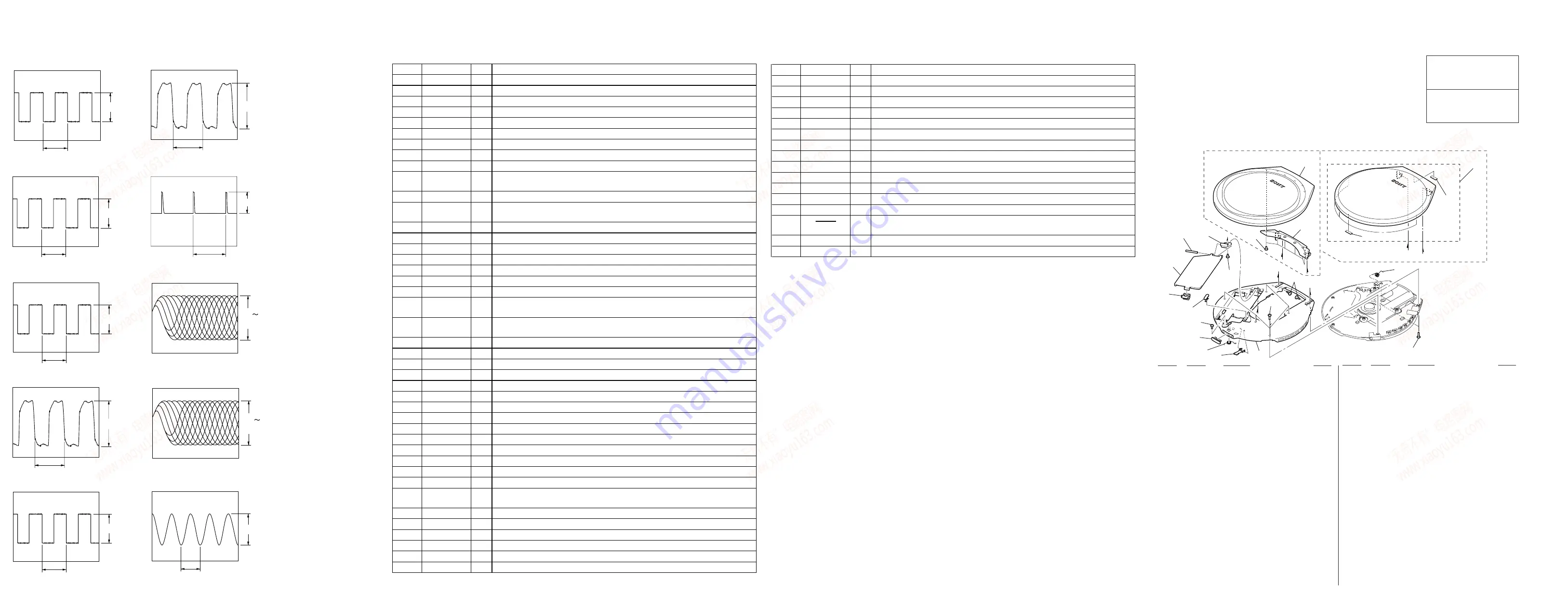
1 V/DIV, 20 µs/DIV

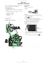
3

IC801 

q;

 MSCK

1 V/DIV, 20 µs/DIV

4

IC801 

ul

 XIN

1 V/DIV, 20 ns/DIV

5

IC601 

wg

 CLOK

1 V/DIV, 20 ns/DIV

6

IC601 

e;

 R4M

1 V/DIV, 20 ns/DIV

7

IC601 

rd

 MDP (CD PLAY)

1 V/DIV, 2 µs/DIV

8

IC601  

tk

 RFDC

100 mV/DIV, 500 ns/DIV

2.0 Vp-p

1.9 

µ

s

2.0 Vp-p

236 ns

2.0 Vp-p

1.9 

µ

s

3.8 

µ

s

2.0 Vp-p

2.0 Vp-p

1.9 

µ

s

400
 600 mVp-p

2.0 Vp-p

236 ns

2.0 Vp-p

1.9 

µ

s

• Waveforms

1

IC402  

9

 CLK

1 V/DIV, 1 µs/DIV

9

IC601 

ua

 RFAC

100 mV/DIV, 500 ns/DIV

q;

IC601 

od

 XTAI

1 V/DIV, 20 ns/DIV

400
 600 mVp-p

2.1 Vp-p

59.0 ns

5-7.

IC  PIN  FUNCTION  DESCRIPTION

15

E888/EJ825

E999/EJ925

15

17

14

13

13

12

11

10

9

6

8

5

4

3

2

1

7

7

16

B

C

C

B

B

C

A

A

17

SECTION  6

EXPLODED  VIEWS

Ref. No.

Part No.

Description

Remark

Ref. No.

Part No.

Description

Remark

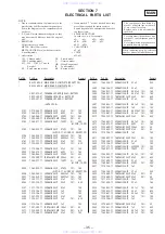
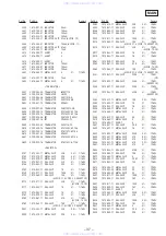
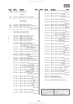
1

X-3380-297-1 CABINET (UPPER) SUB ASSY (E999/EJ925)

1

X-3380-248-1 CABINET (UPPER) SUB ASSY (L) (BLUE)

(E888/EJ825)

1

X-3380-249-1 CABINET (UPPER) SUB ASSY (W) (WHITE)

(E888/EJ825)

1

X-3380-250-1 CABINET (UPPER) SUB ASSY (P) (PINK)

(E888/EJ825)

2

3-221-812-01 LEVER, DETECTION

3

4-224-035-01 SPRING (OPEN)

4

4-224-031-01 KNOB (OPEN)

5

4-908-792-01 SCREW (B2) (SILVER) (E999/EJ925)

*

5

4-908-792-11 SCREW (B2) (BLACK) (E888/EJ825)

6

3-223-889-01 KNOB (AVLS) (E999/EJ925)

6

3-223-889-11 KNOB (AVLS) (DARK BLUE)... (BLUE)

(E888/EJ825)

6

3-223-889-21 KNOB (AVLS) (LIGHT PURPLE)... (WHITE)

(E888/EJ825)

6

3-223-889-31 KNOB (AVLS) (PINK)... (PINK) (E888/EJ825)

7

3-223-826-01 SCREW (B2) (SILVER) (E999/EJ925)

7

4-908-792-91 SCREW (B2) (BLACK) (E888/EJ825)

8

3-221-806-01 SCREW, STEP

9

3-221-811-01 CLAW, LOCK (E999/EJ925)

9

3-221-811-11 CLAW, LOCK (E888/EJ825)

10

3-221-814-01 LID, BATTERY CASE (E999/EJ925)

10

3-221-814-11 LID, BATTERY CASE (E888/EJ825)

11

3-221-815-01 SHAFT (BATTERY CASE LID)

12

3-221-810-01 HINGE, BATTERY CASE LID (E999/EJ925)

12

3-221-810-11 HINGE, BATTERY CASE LID (E888/EJ825)

13

3-318-382-91 SCREW (1.7X2.5), TAPPING

14

3-221-869-01 PLATE, FULCRUM (E888/EJ825)

15

X-3380-251-1 LID SUB ASSY, UPPER (E999)

15

X-3380-252-1 LID SUB ASSY, UPPER (L) (BLUE) (E888)

15

X-3380-253-1 LID SUB ASSY, UPPER (W) (WHITE) (E888)

15

X-3380-254-1 LID SUB ASSY, UPPER (P) (PINK) (E888)

15

X-3380-255-1 LID SUB ASSY, UPPER (EJ925)

(US, CND, E13, HK, KR, CH)

15

X-3380-256-1 LID SUB ASSY, UPPER (EJ925)

(AEP, UK, FR, G, EE)

15

X-3380-257-1 LID SUB ASSY, UPPER (L) (BLUE) (EJ825)

(US, CND, E13, HK, KR, CH)

15

X-3380-258-1 LID SUB ASSY, UPPER (W) (WHITE) (EJ825)

(US, CND, E13, HK, KR, CH)

15

X-3380-259-1 LID SUB ASSY, UPPER (P) (PINK) (EJ825)

(US, CND, E13, HK, KR, CH)

15

X-3380-260-1 LID SUB ASSY, UPPER (L) (BLUE) (EJ825)

(AEP, UK, FR, G)

15

X-3380-261-1 LID SUB ASSY, UPPER (W) (WHITE) (EJ825)

(AEP, UK, FR, G)

15

X-3380-262-1 LID SUB ASSY, UPPER (P) (PINK) (EJ825)

(AEP, UK, FR, G)

16

3-226-920-01 SPRING (FULL OPEN 9) (E999/EJ925)

16

3-226-921-01 SPRING (FULL OPEN 8) (E888/EJ825)

17

3-223-073-01 SPACER (A)

(1)

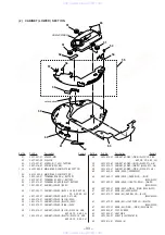
CABINET (UPPER)  SECTION

Les composants identifiés par une
marque 

0

 sont critiquens pour la

sécurité.
Ne les remplacer que par une pièce
portant le numéro spécifié.

The components identified by
mark 

0

 or dotted line with mark

0

 are critical for safety.

Replace only with part number
specified.

• Items marked “*” are not stocked since they

are seldom required for routine service. Some
delay should be anticipated when ordering
these items.

• The mechanical parts with no reference num-

ber in the exploded views are not supplied.

• Accessories and packing materials are given

in the last of the electrical parts list.

NOTE:

• -XX and -X mean standardized parts, so they

may have some difference from the original
one.

• Color Indication of Appearance Parts

Example:
KNOB, BALANCE (WHITE) . . . (RED)

Parts Color Cabinet's Color

• Abbreviation

CH : Chinese model
CND : Canadian model

E13 : 220  – 230 V AC area

in E model

EE

: East European model

 IC801 T5U87-1B68 (SYSTEM CONTROLLER) 

Pin No.

Pin Name

I/O

Description

1

VSS

Ground terminal

2

NC

I

Not used (open)

3

FOK

I

Focus OK signal input from the CXD3028R (IC601)    “L”: NG, “H”: OK

4

AGCPWM

O

AGC control pulse signal output to the power control (IC401)

5

LEDDISP

O

CHG/HOLD LED (D408) ON/OFF control signal output    “L”: lit on

6

NC

O

Not used (open)

7

AMUTE

O

Analog audio muting ON/OFF control signal output terminal    “H”: muting ON

8

VCC2 ON

O

VCC2 voltage control signal output terminal    “H”: ON

9

XRST

O

Reset signal output to the headphone amp (IC351) and CXD3028R (IC601)    “L”: reset

10

MSCK

O

Serial data transfer clock signal output to the power control (IC401), spindle motor driver 
(IC402), and CXD3028R (IC601)

11

MSDTI

I

Serial data input from the CXD3028R (IC601)

12

MSDTO

O

Serial data output to the power control (IC401), spindle motor driver (IC402), and CXD3028R 
(IC601)

13

XWAKEUP

O

Wake-up control signal output (for system standby reset)    “L”: Wake

14

AD SEL

I

Plug-in detection signal input terminal of LINE OUT/OPTICAL OUT (A/D input)

15

AD CHGMNT

I

Battery charge voltage detection input from the power control (IC401) (A/D input)

16

AD VCDKEY2

I

Key input terminal    Not used (Fixed at “H”)

17

AD BATMNT

I

Battery voltage detection signal input terminal

18

AD KEY

I

Key input from the S811 to S816 (

u

.

>

x

/CHG, /–) (A/D input)

19

RMKEY

I

Key input from the headphone with remote commander (A/D input)

20

DCINMNT

I

DC input voltage detection input terminal (A/D input)  and DC input jack use/no use detection 
input terminal (A/D input)

21

WP OPEN

I

CD door open/close detection switch (S801) input
The stop status is reset with the falling edge of input signal

22

VREFL

I

Reference voltage input terminal (0V) for A/D converter

23

VREFH

I

Reference voltage input terminal (+2V) for A/D converter

24

VDD

Power supply terminal (+2V)

25

SCOR

I

Sub-code sync (S0+S1) detection signal input from the CXD3028R (IC601)

26

GRSCOR

I

Communication clock signal input from the CXD3028R (IC601)

27

SPDL MIR/FG

I

FG pulse signal input from the spindle motor driver (IC402)

28

BEEP

O

Beep sound signal output to the headphone amplifier (IC351)

29 to 31

NC

Not used (open)

32

TSB

O

Communication data bus output of headphone with remote commander

33

TEXTSKIP

I

Not used (open)

34

AVOL XAVLS

I

Not used (open)

35

CD RW SEL

I

Not used (open)

36

COMPON

I

G-PRO switch (S805) input     “H”: G-PRO 2

37

DJG TU

I

Not used (open)

38

AVLS

I

AVLS (Automatic Volume Limiter System) switch (S803) input terminal
“L”: normal mode, “H”: limit mode

39

HOLD

I

HOLD switch (S804) input terminal     “L”: hold ON, “H”: hold OFF

40

EX BATT

I

External battery detection signal input terminal

41

DRVRST

O

Reset signal output to the spindle motor driver (IC402)

42

XHGON

O

Optical pick-up power ON/OFF control signal output terminal    “L”: ON

43

XLAT

O

Serial data latch pulse signal output to the CXD3028R (IC601) 

44

XSOE

O

Serial data output enable signal output

Pin No.

Pin Name

I/O

Description

45

DRVLT

O

Latch signal output to the spindle motor driver (IC402)

46

XPOWLT

O

Latch signal output to the power control (IC401)

47

XDOUTON

O

Digital output LED control signal output terminal    “L”: ON

48

XAPC OFF

O

APC muting signal output to the power control (IC401)    “L”: muting

49

NC

Not used (open)

50 to 64

SEG14 to SEG0

O

Segment drive signal output terminal for the display    Not used (open)

65 to 68

COM3 to COM0

O

Common drive signal output terminal for the display    Not used (open)

69 to 71

V3 to V1

O

Bias signal output terminal for the display driver    Not used

72, 73

C1, C0

O

Capacitor connected terminal for the display driver voltage-up (for bias)

74

NC

Not used (fixed at “L”)

75

TEST

I

Test terminal for internal connection (open in this set)

76

XHPSW

O

ON/OFF control signal output to the headphone amp    “L”: ON    Not used (open)

77

XLIGHT

O

Back light control signal output terminal for the display     Not used (open)

78

RESET

I

System reset signal input from the power control (IC401)    “L”: reset
For several hundreds msec. after the power supply rises, “L” is input, then it changes to “H”

79

XIN

I

System clock input from the CXD3028R (IC601)

80

XOUT

O

System clock output terminal    Not used (open)

FR

: French model

G

: German model

HK : Hong Kong model
KR : Korean model

w

w

w

.

x

i a

o

y

u

1

6

3

.

c

o

m

Q

Q

3

7

6

3

1

5

1

5

0

9

9

2

8

9

4

2

9

8

T

E

L

1

3

9

4

2

2

9

6

5

1

3

9

9

2

8

9

4

2

9

8

0

5

1

5

1

3

6

7

3

Q

Q

TEL  13942296513  QQ  376315150  892498299 

TEL  13942296513  QQ  376315150  892498299 

http://www.xiaoyu163.com

http://www.xiaoyu163.com

Summary of Contents for D-E925

Page 1: ...l 220 V 50 Hz Korean model 220 V 60Hz Sony DCC E84 car battery cord for use on car battery 4 5 V DC Battery life approx hours When you use the CD player on a flat and stable surface Playing time varies depending on how the CD player is used When using G PROTECTION 1 2 Two NC 6WM 15 14 charged for about 4 hours Two NC 14WM 29 28 charged for about 4 hours External battery case 50 48 two alkaline bat...

Page 2: ...PLACE THESE COMPONENTS WITH SONY PARTS WHOSE PART NUMBERS APPEAR AS SHOWN IN THIS MANUAL OR IN SUPPLEMENTS PUB LISHED BY SONY TABLE OF CONTENTS 1 SERVICING NOTES 3 2 GENERAL 6 3 DISASSEMBLY 7 4 ELECTRICAL CHECKING 11 5 DIAGRAMS 5 1 Block Diagram MAIN Section 1 2 15 5 2 Block Diagram MAIN Section 2 2 17 5 3 Block Diagram POWER SUPPLY Section 19 5 4 Printed Wiring Board MAIN Board Suffix 11 21 5 5 P...

Page 3: ...f the disc Therefore be sure to keep your eyes more then 30 cm apart from the object lens when you check the emission of laser diode Laser Diode Checking Methods During normal operation of the equipment emission of the laser diode is prohibited unless the upper lid is closed while turning ON the S801 push switch type The following two checking methods for the laser diode are oper able Method Emiss...

Page 4: ... remote commander Optical pickup movement outward or inward Tracking Thread servo OFF PLAYMODE button on remote commander CLV speed becomes 1 to 4 times each time the button is pressed Tracking Thread servo ON PRT ENT buttons on remote commander Tracking gain up mode VOL VOL buttons on the set and VOL VOL knobs on remote commander 2 step volume setting SOUND button on remote commander Servo auto a...

Page 5: ...rror rate is 0 to 99 7350 or NG is displayed when over 100 7350 The remote commander LCD displays the following when no data is read such as in the skip mode Note Press again the DISPLAY button on remote commander and the remote commander LCD displays the time counted down from total time of CD Press once more the DISPLAY button on remote commander and the remote commander LCD returns to the displ...

Page 6: ...s CD player with the remote control supplied with other CD players qh x stop button pages 8 16 ql PLAY MODE button pages 10 12 16 qf Display pages 9 11 15 qk DISPLAY button pages 13 14 wf SOUND button page 14 qg Rotary control N play AMS search pages 8 11 12 AMS search pages 8 11 12 VOL Pull the control in the direction of the arrow and then turn it toward or page 8 w RPT repeat ENT enter button p...

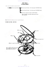
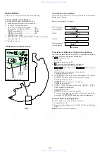
Page 7: ...ng The Battery Terminal Board Relay Lead Wire And Motor Lead Wires 4 five screws B2 5 claw 3 screw B2 2 Open the upper lid sub assy S805 Note on installation cabinet upper section When installing cabinet upper section adjust the S805 and knob AVLS knob AVLS 1 two screws B2 7 spring open 5 two claws 6 cabinet upper section 5 three claws www xiaoyu163 com QQ376315150 9 9 2 8 9 4 2 9 8 TEL 1394229651...

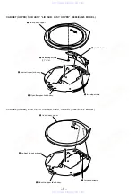
Page 8: ...ssy 2 Open the upper lid sub assy 3 6 plate fulcrum 1 two step screws 5 lid sub assy upper 4 cabinet upper sub assy 2 Open the upper lid sub assy 1 two step screws 3 www xiaoyu163 com QQ376315150 9 9 2 8 9 4 2 9 8 TEL 13942296513 9 9 2 8 9 4 2 9 8 0 5 1 5 1 3 6 7 3 Q Q TEL 13942296513 QQ 376315150 892498299 TEL 13942296513 QQ 376315150 892498299 http www xiaoyu163 com http www xiaoyu163 com ...
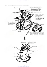
Page 9: ...dhesive sheets and when fixing the optical pick up flexible board do it with two pieces of adhesive sheets as shown in the figure 2 saranet cushion S804 S803 knob HOLD knob AV optical pick up flexible board optical pick up flexible board Note on installation MAIN board When installing MAIN board adjust the S803 S804 and knob AV HOLD two adhesive sheets q spacer MD 6 cushion 7 connector CN503 9 MAI...

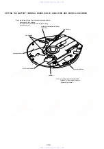
Page 10: ...n figure using saranet cushion Note In routing the motor lead wires fix them to the position shown in figure using cushion two bosses two bosses saranet cushion motor lead wires cushion motor lead wires www xiaoyu163 com QQ376315150 9 9 2 8 9 4 2 9 8 TEL 13942296513 9 9 2 8 9 4 2 9 8 0 5 1 5 1 3 6 7 3 Q Q TEL 13942296513 QQ 376315150 892498299 TEL 13942296513 QQ 376315150 892498299 http www xiaoyu...
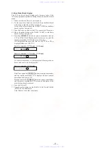
Page 11: ... a disc YEDS 18 3 Press the u button 4 Check the oscilloscope waveform is as shown below A good eye pattern means that the diamond shape in the center of the waveform can be clearly distinguished RF Signal reference Waveform Eye Pattern VOLT DIV 100 mV With the 10 1 probe in use TIME DIV 500 ns To watch the eye pattern set the oscilloscope to AC range and increase the vertical sensitivity of the o...

Page 12: ... TIME REGULATOR CLOCK DIVIDER STATE MACHINE STARTUP PATTERN GENERATOR PATTERN REGULATOR SEQUENCER CPU INTERFACE SERIAL PORT PARALLEL INTERFACE OPERATION MODE OPERATION MODE REGULATOR TEST MODE REGULATOR PREDRIVER FEEDBACK PATTERN GENERATOR BEMF SEPARATOR OVERFLOW REGULATOR PHASE DELAY REGULATOR FEEDBACK RESISTOR PHASE DECODER PWM DECODER FG SYNC PWM POL TEST RST DATA LTCH CLK VC AGND OEB VDU U PGD...

Page 13: ...16 17 18 19 20 21 22 23 24 25 26 27 28 29 30 31 32 33 34 35 36 37 38 39 40 41 42 43 44 45 46 47 48 49 50 51 52 53 54 55 56 57 58 59 60 XOE A0 A11 SYSM AMUTE HPL HPM HPR PCMDI LRCKI BCKI AOUT1 AIN1 LOUT1 LOUT2 AIN2 AOUT2 A9 A8 A7 DVSS RFAC XTAO XTAI XTSL VCTL VPCO WFCK GFS XUGF MDS C2PO WDCK BIAS ASYI ASYO FILO FILI PCO PWMI LOCK MDP SDTI SCSY SCOR SBSO EXCK SDTO XLAT CLOK SENS XSOE R4M IGEN VDD0 C...

Page 14: ...ONTROL ROTATION DETECTOR BEMF SEPARATOR PREDRIVER FEEDBACK PATTERN GENERATOR OR PHASE PWM DECODER 44 MDS 43 MDP 17 SCOR 42 4 1 3 2 23 24 25 14 16 18 20 45 27 22 C176 FOK R4M DRVRST 42 XHGON 39 HOLD 21 WPOPEN XSOE WDCK SDTD SENS CLOK XLAT XSOE XIN GRSCOR FOKI MSDTD SCOR MSDTI MSCK XLAT BUFFER IC403 SYNC 8 9 7 RST DATA LTCH CLK PWM POL FG U1 V1 W1 COM U V W VG VG SPINDLE MOTOR DRIVER IC402 M902 SPIN...

Page 15: ...404 EXTERNAL BATTERY SWITCH Q410 SWITCHING POWER CIRCUIT LENEAR REGULATOR INTERFACE VG POWER CIRCUIT CLK OR OSC 59 47 48 46 49 65 45 CHG SW RF4 INM4 RF21 RF21 RF2 RF2 VCC1 VCPU VLG3 VCPU VCC1 INM2 INM2 APCREF APCREF DTCLD VREF PAPC PA PC WAKEUP LATCH DATA CLOCK DATA CLOCK VLGO2 SYNC 10 9 69 4 3 78 8 52 51 11 18 53 77 57 61 50 79 54 1 72 58 7 SDTO SCK PD 13 LD D F G B A H SYNC DTC2D DTC1D INP1 INP1...

Page 16: ...side seen from Side A the parts face are indicated MAIN board is multi layer printed board However the patterns of intermediate layer have not been included in the diagram Semiconductor Location Suffix 11 and 12 IC602 F 7 IC603 F 6 IC801 H 11 Q301 F 9 Q302 F 9 Q401 I 13 Q402 H 13 Q403 H 12 Q404 H 4 Q405 J 13 Q406 I 2 Q407 G 5 Q408 I 4 Q409 H 15 Q410 G 5 Q411 D 10 Q414 H 14 Q601 F 7 Q602 E 7 Ref No...

Page 17: ...en with aVOM Input impedance 10 MΩ Voltage variations may be noted due to normal produc tion tolerances Waveforms are taken with a oscilloscope Voltage variations may be noted due to normal produc tion tolerances Circled numbers refer to waveforms Signal path J CD PLAY ANALOG OUT c CD PLAY OPTICAL OUT Note The components identi fied by mark 0 or dotted line with mark 0 are criti cal for safety Rep...

Page 18: ...utput L lit on 6 NC O Not used open 7 AMUTE O Analog audio muting ON OFF control signal output terminal H muting ON 8 VCC2 ON O VCC2 voltage control signal output terminal H ON 9 XRST O Reset signal output to the headphone amp IC351 and CXD3028R IC601 L reset 10 MSCK O Serial data transfer clock signal output to the power control IC401 spindle motor driver IC402 and CXD3028R IC601 11 MSDTI I Seria...

Page 19: ... KR CH 59 3 223 810 51 CABINET LOWER PINK EJ825 US CND AEP UK FR G KR CH 59 3 223 810 61 CABINET LOWER BLUE EJ825 E13 HK 59 3 223 810 71 CABINET LOWER WHITE EJ825 E13 HK 59 3 223 810 81 CABINET LOWER PINK EJ825 E13 HK 60 3 221 809 01 KNOB HOLD E999 EJ925 60 3 221 809 11 KNOB HOLD DARK BLUE BLUE E888 EJ825 60 3 221 809 21 KNOB HOLD LIGHT PURPLE WHITE E888 EJ825 60 3 221 809 31 KNOB HOLD PINK PINK E...

Page 20: ...45 01 SHAFT STANDARD 104 4 220 646 01 RACK 105 A 3328 298 A SCREW ASSY FEED 106 3 338 645 31 WASHER 0 8 2 5 107 3 686 458 03 SCREW P1 4X3 5 TAPPING 108 4 220 648 01 GEAR C 109 X 4951 688 1 BRACKET ASSY SLED 110 3 348 998 61 SCREW M1 4X4 TAPPING PAN 111 X 4951 687 1 BASE ASSY SLED M901 A 3328 299 A MOTOR BLOCK ASSY SLED WITH GEAR M902 A 3328 418 A CHASSIS ASSY SPINDLE WITH TURN TABLE 102 110 110 10...

Page 21: ... 10 16V C207 1 164 939 11 CERAMIC CHIP 0 0022uF 10 16V C261 1 125 777 11 CERAMIC CHIP 0 1uF 10 10V C263 1 125 838 11 CERAMIC CHIP 2 2uF 10 6 3V C301 1 117 720 11 CERAMIC CHIP 4 7uF 10V C302 1 115 156 11 CERAMIC CHIP 1uF 10V C303 1 115 156 11 CERAMIC CHIP 1uF 10V C304 1 107 820 11 CERAMIC CHIP 0 1uF 16V C305 1 125 837 11 CERAMIC CHIP 1uF 10 6 3V C306 1 115 156 11 CERAMIC CHIP 1uF 10V C307 1 127 569...

Page 22: ... CERAMIC CHIP 0 001uF 10 16V C801 1 164 943 11 CERAMIC CHIP 0 01uF 10 16V C802 1 125 837 11 CERAMIC CHIP 1uF 10 6 3V C803 1 117 720 11 CERAMIC CHIP 4 7uF 10V C804 1 165 128 11 CERAMIC CHIP 0 22uF 16V C805 1 165 128 11 CERAMIC CHIP 0 22uF 16V C806 1 165 128 11 CERAMIC CHIP 0 22uF 16V C807 1 162 966 11 CERAMIC CHIP 0 0022uF 10 50V C808 1 162 966 11 CERAMIC CHIP 0 0022uF 10 50V C809 1 107 820 11 CERA...

Page 23: ...18 947 11 RES CHIP 330 5 1 16W R206 1 218 945 11 RES CHIP 220 5 1 16W R208 1 218 953 11 RES CHIP 1K 5 1 16W R209 1 218 977 11 RES CHIP 100K 5 1 16W R210 1 218 965 11 RES CHIP 10K 5 1 16W SUFFIX 11 SUFFIX 12 EXCEPT FR R210 1 218 971 11 RES CHIP 33K 5 1 16W SUFFIX 12 FR R211 1 218 953 11 RES CHIP 1K 5 1 16W R212 1 218 953 11 RES CHIP 1K 5 1 16W R261 1 218 929 11 RES CHIP 10 5 1 16W R262 1 218 961 11...

Page 24: ... R627 1 218 990 11 SHORT 0 R629 1 218 887 11 METAL CHIP 47K 0 5 1 16W R630 1 218 937 11 RES CHIP 47 5 1 16W R631 1 218 977 11 RES CHIP 100K 5 1 16W R632 1 218 977 11 RES CHIP 100K 5 1 16W R633 1 218 899 11 METAL CHIP 150K 0 5 1 16W R634 1 218 953 11 RES CHIP 1K 5 1 16W R635 1 218 939 11 RES CHIP 68 5 1 16W R636 1 218 953 11 RES CHIP 1K 5 1 16W R637 1 218 977 11 RES CHIP 100K 5 1 16W R638 1 218 957...

Page 25: ...EDISH EJ925 AEP 3 221 695 61 MANUAL INSTRUCTION PORTUGUESE EJ925 AEP 3 221 695 71 MANUAL INSTRUCTION GERMAN EJ925 AEP G 3 221 695 81 MANUAL INSTRUCTION ITALIAN EJ925 AEP 3 221 695 91 MANUAL INSTRUCTION FINNISH EJ925 AEP 3 221 698 11 MANUAL INSTRUCTION KOREAN EJ925 KR 3 221 698 21 MANUAL INSTRUCTION ENGLISH EJ925 US 3 221 699 11 MANUAL INSTRUCTION CHINESE EJ925 E13 HK 3 221 699 21 MANUAL INSTRUCTIO...

Page 26: ... 1 Printed in Japan C 2000 10 Published by General Engineering Dept www xiaoyu163 com QQ376315150 9 9 2 8 9 4 2 9 8 TEL 13942296513 9 9 2 8 9 4 2 9 8 0 5 1 5 1 3 6 7 3 Q Q TEL 13942296513 QQ 376315150 892498299 TEL 13942296513 QQ 376315150 892498299 http www xiaoyu163 com http www xiaoyu163 com ...

Reviews: