25
D-NE800
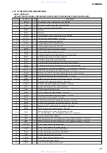
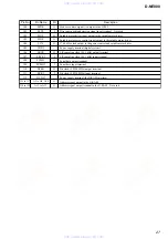
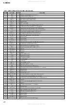
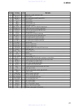
5-10. IC PIN FUNCTION DESCRIPTIONS
Pin No.
Pin Name
I/O
Description
1
XRAS
O
Row address strobe signal output to the D-RAM
2
XWE
O
Data input enable signal output to the D-RAM
3 to 6
D1, D0, D3, D2
I/O
Two-way data bus with the D-RAM
7
DCLK
O
Not used
8
DCKE
O
Not used
9
XCAS
O
Column address strobe signal output to the D-RAM
10
WFCK
O
WFCK signal output terminal Not used
11 to 13
A9 to A7
O
Address signal output to the D-RAM
14
DVSS
—
Ground terminal (for D-RAM interface)
15 to 17
A6 to A4
O
Address signal output to the D-RAM
18
XRDE
I
D-RAM read enable signal input terminal
19
VDD0
—
Power supply terminal (digital system)
20
CLOK
I
Serial data transfer clock input from the system controller
21
SDTO
I
Serial data input from the system controller
22
SENS
O
Serial data output to the system controller
23
XLAT
I
Serial data latch pulse signal input from the system controller
24
XSOE
I
Serial data output enable signal input from the system controller
25
SYSM
I
Analog muting on/off control signal input “H”: muting on Not used
26
WDCK
O
GRSCOR signal output to the system controller Not used
27
SCOR
O
Subcode sync (S0+S1) detection signal output to the system controller
28
XRST
I
Reset signal input from the system controller “L”: reset
29
PWMI
I
Spindle motor external control signal input terminal Not used
30
XQOK
I
Subcode Q OK signal input terminal Not used
31
XWRE
I
D-RAM write enable signal input terminal Not used
32
R8M
O
System clock output to the system controller
33
VSS0
—
Ground terminal (digital system)
34
SQCK
I
SQSO readout clock input terminal Not used
35
SCLK
I
SENS serial data read clock input terminal Not used
36
SQSO
O
CD text data output terminal Not used
O
D-RAM read prohibition signal output terminal Not used
O
D-RAM write prohibition signal output terminal Not used
O
Subcode P to W serial data output terminal Not used
O
SQSO readout clock output terminal Not used
I
Input terminal for the system clock frequency setting
“L”: 16.9344 MHz, “H”: 33.8688MHz (fixed at “L” in this set)
—
Ground terminal (for headphone)
O
PDM signal output for L-ch headphone to the headphone amplifier Not used
O
PDM signal output for R-ch headphone to the headphone amplifier Not used
45
HPVDD
—
Power supply terminal (for headphone)
46
XVDD
—
Power supply terminal (for master clock)
47
XTAI
I
System clock input terminal (16.9344 MHz)
48
XTAO
O
System clock output terminal (16.9344 MHz)
49
XVSS
—
Ground terminal (for master clock)
50
AVDD1
—
Power supply terminal (analog system)
51
AOUT1
O
L-ch analog audio signal output
52
VREFL
O
L-ch reference voltage output terminal
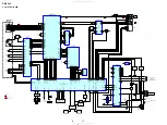
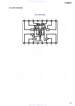
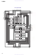
• IC601 CXD3039AR
(RF AMP, DIGITAL SIGNAL PROCESSOR, DIGITAL SERVO PROCESSOR, D-RAM CONTROLLER)
www. xiaoyu163. com
QQ 376315150
9
9
2
8
9
4
2
9
8
TEL 13942296513
9
9
2
8
9
4
2
9
8
0
5
1
5
1
3
6
7
3
Q
Q
TEL 13942296513 QQ 376315150 892498299
TEL 13942296513 QQ 376315150 892498299

