– 11 –
– 12 –
– 13 –
RF level :
0.5
±
0.15 Vp-p
VOLT/DIV : 100 mV (10 : 1 probe in use)
TIME/DIV : 500 nS
SECTION 5
ELECTRICAL ADJUSTMENTS
CD section adjustments are done automatically in this set.
In case of operation check, confirm that focus bias.
5-1. FOCUS BIAS CHECK
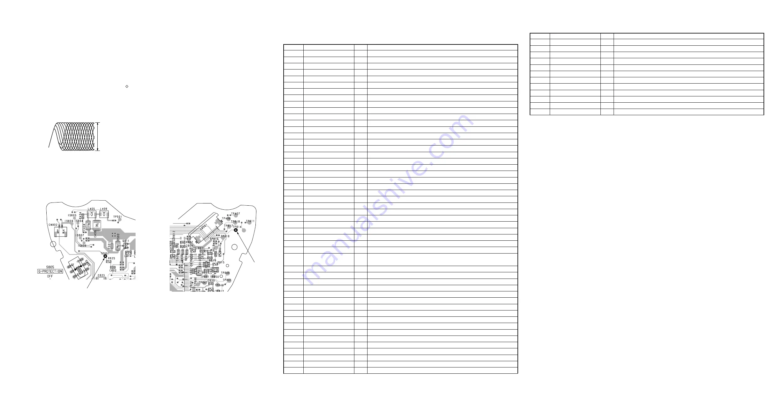
1. Connect the oscilloscope between TP614 (RF) or TP601 (RF)
and GND on main board.
2. Insert the disc (YEDS-18). (Part No. : 3-702-101-01)
3. Press the
u
button.
4. Confirm that the oscilloscope waveform is as shown in the
figure below. (eye pattern)
A good eye pattern means that the diamond shape ( ) in the
center of the waveform can be clearly distinguished.
• RF signal reference waveform (eye pattern)
Test Points:
When observing the eye pattern, set the oscilloscope for AC range
and raise vertical sensitivity.
TP601
– main board (side A) –
– main board (side B) –
TP614
Pin No.
Pin Name
I/O
Pin Description
53 – 56
SEG11 – 8
O
LCD drive segment output (Open)
57 – 64
SEG7 – 0
O
LCD drive segment output (Open)
65 – 68
COM3 – 0
O
LCD drive common output (Open)
69 – 71
V3 – 1
O
LCD drive bias output (Open)
72, 73
C1, 0
O
Capacitor connected terminal of LCD driver for voltage-up.
74
STOP
O
Stop signal output to VCD control IC. (Connect to ground.)
75
TEST
I
Test terminal for IC. Fixed at L.
76
XHPSW (NC)
O
Headphone AMP ON/OFF control signal output. Not used
77
XLIGHT
O
LCD back light control signal output to LCD.
78
RESET
I
System reset signal input from power control IC (IC401). (L: Reset)
79
XIN
I
Oscillation input
80
XOUT
O
Oscillation output (Open)
6-1. IC PIN DESCRIPTION
• IC801 TMP88CM22F (SYSTEM CONTROLLER)
Pin No.
Pin Name
I/O
Pin Description
1
VSS
I
Ground
2
IRRMC
I
Fixed at L.
3
FOKI
I
Focus OK signal input from digital servo processor (IC601).
4
AGCCON
O
AGC control pulse output
5
XLEDDISP
O
CHG/HOLD LED control signal output
6
VCC SWITCHING
O
Control signal output for Switching power supply circuit.
7
AMUTE
O
Analog audio muting ON/OFF signal control signal output (H: Mute ON)
8
VCC2 ON
O
VCC2 voltage control output
9
XRST
O
Reset signal output to CXD3027R (IC601). (L: Reset)
10
SCK
O
Serial data transfer clock signal output to CXD3027R (IC601).
11
SDTI
I
Serial data input from CXD3027R (IC601).
12
SDTO
O
Serial data output to CXD3027R (IC601).
13
SLPOUT
O
WAKE-UP control signal output (for system standby reset)
14
SEL
I
Plug-in detection signal input of LINE OUT/OPTICAL OUT jack.
15
CHGMNT1
I
Battery charge voltage detection input from power control IC (IC401).
16
VCDKEY
I
Fixed at H.
17
BATMNT
I
Battery voltage detection input
18
KEY
I
Key input from switch unit (A/D input)
19
RMKEY (NC)
I
Key input from headphones with remote controller (A/D input). Fixed at L.
20
DCINMNT
I
DC input voltage detection input (A/D input) DC input jack use/no-use detect input
21
OPEN
I
CD door open/close detection input
22
VREFL
I
Reference voltage (0 V) input for A/D converter.
23
VREFH
I
Reference voltage (+2 V) input for A/D converter.
24
VDD
—
Power supply pin (+2 V)
25
SCOR
I
Sub code sync detection input from CXD3027R (IC601).
26
GRSCOR
I
GRSCOR signal input
27
FG
I
FG pulse input
28
BEEP
O
Beep sound output to headphone AMP (IC351).
29
NC
—
Not used. (Open)
30
RMSCK (NC)
O
Communication clock. Not used.
31
RMDATI (NC)
I
Communication data bus of headphones with remote controller. Not used.
32
RMDATO (NC)
O
Communication data bus of headphones with remote controller. Not used.
33
RMRW (NC)
O
Read/write control signal output to headphones with remote.
(L: Read, H: Write) Not used.
34
RMLAT (NC)
O
Serial data latch pulse output to headphones with remote. Not used.
35
WFCKI
I
WFCK input
36
COMPON I
I
Key input from G-protection switch (S805).
37
XNTSC I
I
Not used. Fixed at H.
38
AVLS
I
AVLS (Automatic Volume Limiter System) switch input (L: Normal, H: Limit)
39
HOLD
I
HOLD switch input (L: HOLD on, H: HOLD off)
40
EX BATT (NC)
I
EXT BATT plug-in detection input Not used
41
DRVRST
O
Spindle motor driver control signal output
42
XOE
O
Optical pick-up VCC control signal output (L: on)
43
XLAT
O
Serial data latch pulse output to D-RAM controller (IC601). (for ESP)
44
XSOE
O
Output enable signal output (for ESP)
45
DRVLT
O
Spindle motor driver latch output
46
XPOWLT
O
Latch output to VCD control IC.
47
XDOUTON (NC)
O
DIGITAL OUT LED control signal output Not used
48
XAPC OFF
O
APC mute signal output (L: mute)
49
XVRST (NC)
—
Not used. (Open)
50 – 52
SEG14 – 12
O
LCD drive segment output (Open)
SECTION 6
DIAGRAMS


