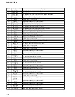
103
DVP-CX777ES
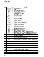
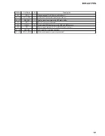
Pin No.
Pin Name
I/O
Description
49
AVDREQ1
I
Request signal input from the AV decoder
50
AVDDACK1
O
Acknowledge signal output to the AV decoder
51
XIFCS
O
Chip select signal output to the interface controller
52
VSS
—
Ground terminal
53
X1
O
System clock output terminal (16.5 MHz)
54
X0
I
System clock input terminal (16.5 MHz)
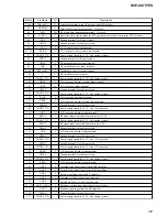
55
VCC
—
Power supply terminal (+3.3V)
56
(CKSW1)
O
Not used
57
(OCSW1)
O
Not used
58
XROMCS
O
Chip select signal output to the flash memory
59
XRAMCS
O
Chip select signal output to the S-RAM
60, 61
XAVCS0, XAVCS1
O
Chip select signal output to the AV decoder
62
XARPCS
O
Chip select signal output to the DSP
63
XSDSPCS
O
Chip select signal output to the DSP
64
VCCI
—
Power supply terminal (+1.8V)
65
XGACS
O
Chip select signal output to the mechanism controller
66
(NC)
O
Not used
67
XWAIT
I
Wait signal input from the DSP and AV decoder
68
TEST (H)
I
Input terminal for the test (normally: fixed at “H”)
69
TEST
I
Input terminal for the test
70
XRD
O
Read enable signal output to the flash memory, S-RAM, DSP, AV decoder and mechanism
controller
71
XWRH
O
High byte write enable signal output to the flash memory, S-RAM, DSP, AV decoder and
mechanism controller
72
XWRL
O
Low byte write enable signal output to the S-RAM
73
XNMI
I
Not used
74
VCCI
—
Power supply terminal (+1.8V)
75
VSS
—
Ground terminal
76
XRESET
I
Reset signal input from the interface controller “L”: reset
77
CPUCK
O
Master clock (33 MHz) signal output to the mechanism controller
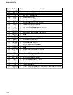
78
SMUTE
O
Soft muting control signal output to the DSD decoder
79
XDACS
O
Chip select signal output to the D/A converter
80
XADSPCS
O
Chip select signal output to the audio DSP
81
48/44.1K
O
PLL frequency control signal output to the clock generator
82
XLDON
O
Laser diode control signal output to the RF amplifier
83
MAMUTE
O
Audio muting control signal output terminal
84
XSRWE
O
Write enable signal to the S-RAM
85 to 100
HD0 to HD15
I/O
Two-way data bus terminal
101
VSS
—
Ground terminal
102 to 109
HA0 to HA7
O
Address signal output terminal
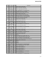
110
VCC
—
Power supply terminal (+3.3V)
111 to 118
HA8 to HA15
O
Address signal output terminal
119
VSS
—
Ground terminal
120
HA16
O
Address signal output terminal


