background image

2-2

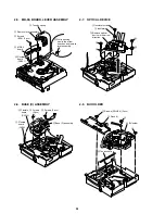
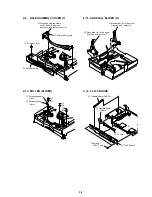
2-5. MD-90, BOARD, LEVER ASSEMBLY

2-6. BASE (C) ASSEMBLY

2-7. OPTICAL DEVICE

2-8. BU HOLDER

1

 Tension spring

2

 While pushing

     claw in the arrow
     direction, and remove
     lever assembly.

3

 Remove lever assembly.

4

 Flexible

     board
     (CN301)

5

 Screws

     (B2.6) (2 pcs)

6

 MD-90

     board

1

 Flexible

     board
     (CN102)

2

 Flexible

     board
     (CN103)

3

 Screws

     (2 pcs)

4

 Screws (2 pcs)

5

 Base (C) assembly

3

1

3

1

1

 Insulator screw

2

 Remove optical

     device in the arrow
     direction.

3

 Insulator

1

1

1

 Screws (PWH 2.6) (3 pcs)

2

 BU holder

3

 Rack (L)

4

 Tension spring

Summary of Contents for DVP-F21 - Cd/dvd Player

Page 1: ...5 kg 3 lb 5 oz Operating temperature 5 C to 35 C 41 F to 95 F Operating humidity 25 to 80 Jack name Jack type Maximum output level Load impedance DIGITAL OUT OPTICAL Optical output jack 18 dBm Wave length 660 nm AUDIO OUT L R Phono jack 2 Vrms 50 kilohms Over 10 kilohms VIDEO OUT Phono jack 1 0 Vp p 75 ohms sync negative S VIDEO OUT 4 pin mini DIN Luminance signal 1 0 Vp p Color signal 0 286 Vp p ...

Page 2: ...multimeter is suitable for this job 3 Measuring the voltage drop across a resistor by means of aVOM or battery operated AC voltmeter The limit indica tion is 0 75V so analog meters must have an accurate low voltage scale The Simpson 250 and Sanwa SH 63Trd are ex amples of a pas sive VOM that is suitable Nearly all battery operated digital multimeters that have a 2V AC range are suit able See Fig A...

Page 3: ...CESS Schematic Diagram 4 21 MB 99 POWER Schematic Diagram 4 23 MB 99 AV OUT Schematic Diagram 4 25 MB 99 VIDEO Schematic Diagram 4 27 MB 99 AUDIO Schematic Diagram 4 29 MB 99 AVMS Schematic Diagram 4 31 MD 89 FUNCTION SWITCH 1 Printed Wiring Board and Schematic Diagram 4 33 FL 123 INTERFACE CONTROL Printed Wiring Board 4 35 FL 123 INTERFACE CONTROL Schematic Diagram 4 37 MD 90 FUNCTION SWITCH Prin...

Page 4: ......

Page 5: ...software producers Since this player plays DVDs and VIDEO CDs according to the disc contents the software producers designed some playback features may not be available Also refer to the instructions supplied with the DVDs or VIDEO CDs Copyrights This product incorporates copyright protection technology that is protected by method claims of certain U S patents other intellectual property rights ow...

Page 6: ...s 37 K H PLAY button 36 L TOP MENU button 39 M DISPLAY button 66 N TV DVD switch 64 O 1 power button 36 P TV operation buttons 64 Q SUBTITLE button 55 R CLEAR button 41 43 44 44 S VOL volume buttons 64 T A B button 44 U REPLAY button 37 V SCAN SLOW buttons 46 wd x STOP button 37 wf X PAUSE button 37 wg MENU button 39 wh C X x c buttons 32 wj ORETURN button 40 wk ENTER button 32 13 Guide to On Scre...

Page 7: ...hen using the remote point it at the remote sensor on the player Continued 16 If you cannot operate the player with the remote The player has 2 remote sensors one at the top and one on the front page 18 If one of the remote sensor is exposed to direct sunlight or lighting apparatus the remote may not operate correctly If this happens select a remote sensor in the following way until you find one t...

Page 8: ...ted noise Refer to the instructions supplied with the components to be connected 20 Step 1 Connecting the Video Cords Connect this player to your TV monitor projector or AV amplifier receiver using a video cord Select one of the patterns A or B according to the input jack on your TV monitor projector or AV amplifier receiver Audio video cord supplied S video cord not supplied CD DVD player AC powe...

Page 9: ...is used for video signals page 20 A Audio video cord supplied CD DVD player TV white red yellow white red yellow l Signal flow to audio input to AUDIO OUT L to AUDIO OUT R AC power cord supplied AC power adaptor AC F21 supplied white red continued 24 Connecting to a stereo amplifier receiver and 2 speakers Connecting to an MD deck or DAT deck This connection will use your 2 front speakers connecte...

Page 10: ...plied to optical digital input white red white red Amplifier receiver with Dolby Surround decoder Speakers Speakers Rear L Rear R Subwoofer Center Rear mono Front L Front R l Signal flow or to AUDIO OUT R to AUDIO OUT L to DIGITAL OUT OPTICAL AC power adaptor AC F21 supplied AC power cord supplied white red continued 28 Connecting to an AV amplifier receiver with a digital input jack having a Dolb...

Page 11: ...he player down from the wall Step 4 Connecting the Power Cord Plug the player and TV power cords into an AC outlet Do not connect the power cord of your player to the switched power socket of an amplifier receiver Otherwise when you turn off the power of your amplifier receiver the settings for the player may be lost 3 1 4 in 3 16 7 32 in 32 Step 5 Quick Setup Follow the steps below to make the mi...

Page 12: ...eractively by following the instructions on the menu DVD page 39 VIDEO CD page 40 To turn off the player Press 1 The player enters standby mode and the 1 indicator lights up in red To turn off the player completely disconnect the AC power cord While playing a disc do not disconnect the AC power cord Doing so may cancel the menu settings When you turn off the player first press x to stop playback a...

Page 13: ...em you want to change 3 To change other items repeat Step 2 4 Press ENTER TOP MENU C X x c ENTER C X x c MENU ENTER 40 Playing VIDEO CDs with PBC Functions PBC Playback With PBC Playback Control functions you can enjoy simple interactive operations search functions and other operations PBC playback allows you to play VIDEO CDs interactively by following the menu on the TV screen 1 Start playing a ...

Page 14: ...he player shuffle titles chapters or tracks and play them in a random order Subsequent shuffling may produce a different playing order 1 Press SHUFFLE during playback The Control Bar is displayed 2 Press SHUFFLE repeatedly to select the item you want to set x When playing a DVD Program Play is set to OFF TITLE Shuffles titles and plays them in random order CHAPTER Shuffles chapters and plays them ...

Page 15: ... of the title track scene time code etc you want by pressing X x to select the digit following by c to move the cursor For example to find the scene at 2 hours 10 minutes and 20 seconds after the beginning select TIME TEXT in Step 2 and enter 2 10 20 If you make a mistake Cancel the number by pressing CLEAR then select another number 4 Press ENTER The player starts playback from the selected numbe...

Page 16: ...r discs not in multiple audio format you cannot change the sound While playing a DVD the sound may change automatically AUDIO DISPLAY 1 4 ENGLISH continued 52 Checking the audio signal format If you press DISPLAY twice during playback the format of the current audio signal Dolby Digital DTS PCM etc appears as shown below Example Dolby Digital 5 1 ch Dolby Digital 3 ch PCM Stereo About audio signal...

Page 17: ... train s movement interrupted 1 Press ANGLE during playback The Control Bar is displayed The number in parentheses indicates the total number of available angles 2 Press ANGLE repeatedly to select the angle number The scene changes to the selected angle Note Depending on the DVD you may not be able to change the angles even if multi angles are recorded on the DVD Displaying the Subtitles If subtit...

Page 18: ... CUSTOM PARENTAL CONTROL display appears 2 Enter your 4 digit password using X x to select the digit followed by c to move the cursor Then press ENTER The player is ready for playback z If you forget your password enter the 6 digit number 199703 when the CUSTOM PARENTAL CONTROL display asks you for your password then press ENTER Press c after the 4th digit to allow the entire 6 digit number to be ...

Page 19: ...move the disc 2 Press and hold X on the player for more than two seconds You will hear one beep and the Sound Feedback function is turned on To turn off the Sound Feedback function When there is no disc in the player press and hold X on the player for more than two seconds You will hear two beeps and the Sound Feedback function is turned off Operation Operation sound Power is turned on One beep Po...

Page 20: ...e language of the subtitles recorded on the DVD Select the language from the displayed list When you select AUDIO FOLLOW the language for the subtitles changes according to the language you selected for the sound track SCREEN SETUP TV TYPE SCREEN SAVER BACKGROUND 4 3 LETTER BOX 4 3 LETTER BOX 4 3 PAN SCAN 16 9 Options SCREEN SETUP TV TYPE SCREEN SAVER BACKGROUND 16 9 ON JACKET PICTURE Selected set...

Page 21: ...CM in DIGITAL OUT page 73 xDOWNMIX DVD only Switches the mixing down methods when you play a DVD on which rear signal components such as Rear L Rear R or Rear Monaural are recorded in Dolby Digital format For details on the rear signal components see Changing the Sound page 51 This function affects the output of the following jacks AUDIO OUT L R jacks DIGITAL OUT OPTICAL jack when DOLBY DIGITAL is...

Page 22: ...ont panel display page 10 The DVD prohibits changing of the angles continued 76 The player does not operate properly When static electricity etc causes the player to operate abnormally disconnect the AC power cord once then connect it again Nothing is displayed on the front panel display DIMMER in CUSTOM SETUP is set to OFF Set DIMMER to BRIGHT or DARK page 70 If you set to AUTO the display turns ...

Page 23: ...O OUT 4 pin mini DIN Luminance signal 1 0 Vp p Color signal 0 286 Vp p 75 ohms sync negative 75 ohms terminated continued 80 AC power adaptor Model name AC F21 Power requirements 100 to 240 V AC 50 60 Hz Output voltage DC 10 5 V 1 3 A in operating mode Operating temperature 5 C to 35 C 41 F to 95 F Storage temperature 20 C to 60 C 4 F to 140 F Supplied accessories See page 15 Optional accessory Ac...

Page 24: ...ROUND 69 Batteries 15 BNR 56 C CD 36 CHAPTER 47 Chapter 77 Connecting 19 Continuous Play CD VIDEO CD DVD 36 Control Bar 14 Control Menu 14 CUSTOM 66 CUSTOM PARENTAL CONTROL 58 CUSTOM SETUP 70 D DIGITAL OUT 72 Digital output 24 72 DIMMER 70 Display Control Menu Display 14 Front Panel Display 10 Setup Display 66 DOLBY DIGITAL 51 73 DOWNMIX 72 DTS 51 DVD 36 77 DVD s menu 39 F Fast forward 37 Fast rev...

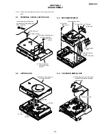
Page 25: ...pcs 4 Screws 3 pcs 5 Remove case lower in the arrow direction 2 Feet 2 pcs Insert the small type flat blade screwdriver into the groove and lift up rubber foot 5 Remove case upper in the arrow direction 4 Claw 3 Claw 2 Claw 1 Claw 1 Ground plate rear 2 Ground plate side 3 Flexible boards 3 pcs CN201 202 402 4 Screws B3 2 pcs 5 Screw B3 6 Mechanism deck 2 While opening claw in the arrow direction a...

Page 26: ...and remove lever assembly 3 Remove lever assembly 4 Flexible board CN301 5 Screws B2 6 2 pcs 6 MD 90 board 1 Flexible board CN102 2 Flexible board CN103 3 Screws 2 pcs 4 Screws 2 pcs 5 Base C assembly 3 1 3 1 1 Insulator screw 2 Remove optical device in the arrow direction 3 Insulator 1 1 1 Screws PWH 2 6 3 pcs 2 BU holder 3 Rack L 4 Tension spring ...

Page 27: ...wo claws on the base in the arrow directions and remove cover T 4 Compression spring 1 2 1 2 1 2 1 Stopper washers 4 pcs 2 Rollers slider 4 pcs 2 Move slider L in the arrow direction and remove it 1 Move slider R in the arrow direction and remove it 5 FL 123 board 1 FL cover 2 Flexible board CN403 3 Flexible board CN404 4 Screws B3 2 pcs ...

Page 28: ...39 board 3 Screws B3 4 pcs 4 Screws B3 4 pcs 5 Screws B3 3 pcs 6 MB 99 board 2 14 Sliders L and R Phase Adjustment When installing the gear P the phase adjustment between sliders L and R is performed in the following position 1 Gear P Slider R Slider L ...

Page 29: ...2 5 2 15 INTERNAL VIEWS ...

Page 30: ...2 16 CIRCUIT BOARDS LOCATION IR 39 IR FL 123 INTERFACE CONTROL MD 89 FUNCTION SWITCH 1 MD 91 MB 99 VIDEO AUDIO SIGNAL PROCESS SERVO MD 90 FUNCTION SWITCH 2 2 6 E ...

Page 31: ... AU 11V AI 5V SW 11V 11V 3 3V 1 8V 5V ND402 IC403 IF CON IC103 CDDOUT CDDATA CDBCK CDLRCK IC302 KATRINA SD 0 7 RF IC503 AV DECODER IC303 16M DRAM IC504 16M SDRAM IC108 OTP IC101 8K EEP ROM IC107 16M FLASH IC802 AUDIO D A CONVERTER SPDIF Parallel BUS VIDEO V VIDEO Y VIDEO C ACH12 ACH34 ACH56 BCK LRCK IC801 AUDIO DSP AUDIO AMP AUDIO LT AUDIO RT VIDEO BUFFER IC902 IC1003 IC1001 IC601 BNR VIDEO S VIDE...

Page 32: ...96 197 173 175 180 185 144 172 142 143 166 204 205 46 1 202 203 139 140 ADC1 ADC0 ADC2 MIRR TZC DFCTI ADC7 GIO5 PGIN ADC5 6 GIO0 INT2 POM2 3 POM0 1 ADC3 ADC4 GIO7 SDO GIO8 SCK GIO13 GIO6 SDI HINT 22 HCS 24 XD SPRST 156 167 168 200 196 199 159 161 176 177 GI01 INT3 PWM0 1 GIO2 INT4 PWM2 GIO9 FGREF GIO10 FGIN MDSO MDPO CN202 CN201 XSDPIT XSDPCS XRST XD RVMUTE SYSTEM CONTROL SEE PAGE 3 7 XL DON OPTIC...

Page 33: ...60 VREFI 84 HSYNCO 88 NRSENB 113 NRSDOUT 112 FLDO 87 G OUT 69 R OUT 63 B OUT 66 COMPOUT 80 Y OUT 74 C OUT 77 100 97 95 92 PDI 0 7 124 125 127 128 130 133 131 134 136 137 139 140 160 157 165 162 173 167 174 168 176 170 177 171 146 144 147 151 149 125 155 154 143 XSRQ XSAK SDEF SDCK XSHD CDDATA CDBCK CDLRCK CDDOUT SDI 0 7 HA 0 7 HD 8 15 HA 0 7 HA 0 7 PDI 0 7 PDO 0 7 HA 0 21 HD 0 15 XRD XWRH ACH12 AC...

Page 34: ...1 X39CS XVESCS MAMUTE XDACS 81 48 44 1K WIDE 82 WIDE WIDE INTERFACE CONTROL VIDEO TRST XRST FSEL 14 33 1OUT 15 33 2OUT 13 27 1OUT 3 XT1 7 XT0 8 512 2OUT 9 512 1OUT 10 16 5MHz X101 X102 27MHz 512FS6CH IC102 PLL 512FSAVD 27MAVD 33MAVD 33MARO 512FS2CH AUDIO SEE PAGE 3 9 10 HD 0 15 HA 0 21 IC107 FLASH IC108 OTP or MB 99 BOARD 3 4 SIGNAL PROCESSOR CN104 SYSTEM IC103 CONTROL SEE PAGE 3 4 RF SEFVO SIGNAL...

Page 35: ...H 12 IC902 0 7Vp p H 15 IC902 0 7Vp p H 17 IC902 SEE PAGE 3 5 6 3 6 AUDIO BLOCK DIAGRAM ACH12 6 SDI0 ACH34 7 SDI1 ACH56 8 SDI2 LRCK 5 LRCKI BCK 9 BCKI SC1 SO1 S 1 X39CS XVESCS 512FS6CH SO 17 14 13 SCK SI 11 3 XCS MCLK XRST 48 XRST 37 SDO0 3 SDTI 4 2 LRCK BICK PDN 5 8 7 CDTI CCLK 6 1 CSN MCLK AOUTL 12 11 AOUTL 10 AOUTR 9 AOUTR 16 DZFL 6 5 2 3 7 1 AUDIO DSP IC801 AUDIO D A CONVERTER IC802 AUDIO AMP ...

Page 36: ... IN 10 5V L703 D705 CN40 PS701 PS702 PS703 PS704 SEE PAGE 4 23 24 SEE PAGE 4 6 SEE PAGE 4 37 38 3 11 3 12 E 3 7 INTERFACE CONTROL BLOCK DIAGRAM 14 SI0 SI0 16 SO SO0 13 SO0 SI 15 SC0 12 SC0 SC 17 XIFCS 15 XIFCS CS 14 XIFBUSY 16 XIFBUSY BUSY 27 XFRRST 10 XFRRST FRRST 7 A MUTE 8 AMUTE 28 V MUTE 7 VMUTE 29 XDISC 1 DISC 13 XINS 3 INS 25 CN403 CN403 CN403 LED5 41 BNR 79 SURROUND D415 RST 8 65 46 SEG 1 1...

Page 37: ...s 1 4 W Chip resistors 1 10 W un less otherwise specified kΩ 1000Ω MΩ 1000kΩ All capacitors are in µF unless otherwise noted pF µµF 50V or less are not indicated except for electrolytics and tantalums All variable and adjustable resistors have characteristic curve B unless otherwise noted nonflammable resistor fusible resistor panel designation f internal component adjustment for repair B Line B L...

Page 38: ...P RM 2 3 ROSW1 ROSW2 11 11 ROSW2 3 3V_MNT 1 18 3 3V_MNT RM 1 4 GND ROSW3 10 10 ROSW3 XFRRST 2 17 XFRRST CN402 ROSW4 9 9 ROSW4 XIFBUSY 3 16 XIFBUSY RM 1 RM ROSW1 8 8 ROSW1 XIFCS 4 15 XIFCS RM 2 RM GND 7 7 GND SIO 5 14 SIO MD 091 RM 6 6 RM SOO 6 13 SOO CN104 RM 5 5 RM SCO 7 12 SCO CKM 1 CKM CKSW3 4 4 CKSW3 GND 8 11 GND CKM 2 CKM CKSW2 3 3 CKSW2 IFRST 9 10 IFRST LVSW1 2 2 LVSW1 PCONT 10 9 PCONT CN301...

Page 39: ...RWAKE IC1651 REMOTE CONTROL RECEIVER FL 123 BOARD CN404 4 5 4 6 IR IR 39 4 2 PRINTED WIRING BOARDS AND SCHEMATIC DIAGRAMS IR 39 IR PRINTED WIRING BOARDS AND SCHEMATIC DIAGRAMS Ref No IR 39 board 50 000 series C1651 C1652 C1653 CN1651 CN1652 CN1653 IC1651 L1651 R1651 R1653 R1654 R1656 R1657 R1659 IR 39 BOARD SIDE A 1 682 756 11 11 08 R1652 R1655 R1658 IR 39 BOARD SIDE B 1 682 756 08 11 11 A B C D E...

Page 40: ...022 R1026 R1030 R1034 R1036 R1037 R1045 R1046 R1047 R1049 R105 R108 R110 R1101 R1102 R1105 R1106 R1108 R1115 R1116 R112 R1124 R1125 R113 R1134 R1143 R1144 R1148 R1149 R1156 R119 R1208 R1212 R122 R123 R139 R143 R145 R159 R163 R164 R165 R166 R167 R170 R177 R178 R179 R180 R181 R196 R197 R205 R237 R301 R302 R305 R306 R307 R308 R309 R310 R311 R312 R316 R317 R318 R320 R324 R325 R326 R339 R340 R365 R368 ...

Page 41: ...2 R1153 R1154 R1155 R1157 R1158 R1159 R116 R1160 R1161 R1162 R1163 R1164 R1165 R1166 R1167 R1168 R1169 R117 R1170 R1171 R118 R1209 R121 R1210 R1211 R128 R129 R130 R134 R135 R136 R137 R138 R140 R141 R142 R144 R146 R147 R148 R149 R150 R151 R152 R153 R154 R155 R156 R157 R158 R160 R161 R162 R168 R169 R171 R172 R175 R176 R182 R195 R201 R202 R203 R204 R207 R208 R209 R210 R211 R212 R213 R214 R215 R216 R2...

Page 42: ...10 13 14 15 16 17 18 19 20 21 22 23 24 25 26 27 28 29 30 31 32 35 36 37 38 39 40 11 12 33 34 41 42 43 44 FL103 0 01u B C133 XX IC109 1 2 3 4 5 6 7 8 9 10 13 14 15 16 17 18 19 20 21 22 23 24 25 26 27 28 29 30 31 32 35 36 37 38 39 40 11 12 33 34 41 42 43 44 FL109 0 01u B C124 XX R162 MBM29LV160BE 90TN IC107 1 2 3 4 5 6 7 8 9 10 11 12 13 14 15 16 17 18 19 20 21 22 23 24 25 26 27 28 29 30 31 32 33 34 ...

Page 43: ...2 T100 QR Q202 47uH L202 47uH L201 XX R236 33 R207 0 01u B C224 16V 10u C209 33 R223 XX D204 0 01u B C218 2 2M R238 6 3V 47u C217 6 3V 47u C223 0 01u B 16V 10u C221 47k R225 0 R205 B2 C2 D2 D C B A E F MIRR SSDFCTI TZC PI TE FE SSCK SSWD SSRD SSCS TRK TRK FCS FCS INLIM SLB SLA SLB SLA SPM SPM SS_MON XDRVMUTE SVC RFTPON 0 01u B C246 XX C249 27k R244 JL231 100k R243 0 1u B C247 0 1u B C243 XX C251 0...

Page 44: ...S XRAS XOE VDD 1 8V MD0 MD1 MD3 MD2 MD4 MD5 MD7 MD6 VSS XDSPRST TESTK2 TESTK1 TESTK0 VSS VRTA TESTAA VSSA0 VRBA VSSD0 VDDA0 3 3V ADC7 ADC6 ADC5 VSSA0 ADC4 ADC3 ADC2 ADC1 ADC0 VDDD1 3 3V VSSD1 VRB RFIN1 VSSA1 AIN RFIN2 VRT VDDD2 3 3V VSSD2 IREF AOUT VSSA2 BIAS VREF Y FR1 FR2 FR3 INM INP VSSA3 R2 R1 VCO VSSA4 VSS ADO7 ADO6 ADO5 ADO4 ADO3 ADO2 ADO1 ADO0 PLCKO VSS RFD VDD 1 8V ESTB MNT7 MNT6 MNT5 MNT4...

Page 45: ...R423 470k R426 10k R413 D IN3 OUT3 IN4 IN5 MUTE34 TSD M MUTE12 MUTE12 MUTE5 MUTE5 TSD M SGND MSC IN5 REV DO6 MUTE34 PVCC2 D PGND2 CTL OUT4 IN4 OUT5 FWD SW SPDL R434 330 10k R433 0 5 56k R431 XX C417 33k R419 33k R418 0 01u B C416 100p C403 120k R407 33k R422 220p C402 FAN8034 IC401 1 2 3 4 5 6 40 41 42 43 44 45 46 47 48 52 37 38 39 0 5 56k R429 220p C407 10k R432 XX C425 0 033u B C412 150k R408 0 ...

Page 46: ...504 1 2 3 4 5 6 7 8 9 10 11 12 13 14 15 16 17 18 19 20 21 22 23 24 25 26 27 28 29 30 31 32 33 34 35 36 37 38 39 40 41 42 43 44 45 46 47 48 49 50 MSM56V16160F 10TS K IC505 1 2 3 4 5 46 47 48 49 50 0 01u B C526 0 01u B C531 10 R533 XX R532 XX C544 XX C532 ADDT2 ADDT14 ADDT2 ADDT1 ADDT13 ADDT15 ADAD6 ADAD2 ADDT3 ADAD0 ADAD5 ADAD9 ADAD7 ADDT12 ADAD10 ADAD3 ADAD4 ADAD1 ADDT6 ADAD8 ADDT5 ADAD11 ADDT15 A...

Page 47: ... 8 11 MB 99 BOARD 5 11 MB 99 BOARD 1 11 H_SYNC NRSDIN SCS GND CK27 VDD MRST FID YCOUT0 YCOUT1 YCOUT2 GND VDD YCOUT3 YCOUT4 YCOUT5 YCIN_6 YCIN_7 EXPH1 EXPH0 YCOUT7 YCOUT6 TMC YCIN_5 YCIN_4 YCIN_3 GND YCIN_2 YCIN_1 YCIN_0 PDI0 PDI1 PDI2 PDI3 PDI4 PDI5 PDI6 PDI7 FLD CSVGA DATAVGA 27MVGA32 XRST PDI0 PDI1 PDI2 PDI3 PDI4 PDI5 PDI6 PDI7 VDD GND IC601 BNR 1 0 B B B 1 6 1 7 3 3 1 4 1 3 1 2 0 0 0 0 0 0 3 1 ...

Page 48: ... 0 R748 0 1u B C745 470 R756 0 R749 0 001u B C717 XX R723 XX R724 0 5 10k R710 XX R726 0 5 10k R711 100k R755 R720 10k BA9743AFV E2 IC701 1 2 3 4 5 6 7 8 9 10 11 12 13 14 15 16 TL594CPWR IC702 1 2 3 4 5 6 7 8 9 10 11 12 13 14 15 16 0 01u B C713 0 1u B C706 47k R712 470p B C711 7500 R751 0 1u B C708 XX C715 0 01u B C712 68k R709 0 1u B C710 3300p B C714 33k R746 10k R727 3900 R754 0 1u B C705 XX C7...

Page 49: ...1 SDI2 BCKI VSS XCS N C SI SCK VDD VSS SO B15 VSS 1 2MCLK B14 B13 B12 B11 B10 B00 B01 B08 B09 B03 B02 B04 B07 B06 B05 VSS VDD LRCK ACH12 ACH34 ACH56 BCK XVESCS SC1 XDACS SO1 XRST 3 3V GND SI1 512FS6CH 512FS2CH LRCK0 SDT0 BCK0 SDTI0 LRCKI0 MCLKI0 BCKI0 XDACS0 DSP_SC0 DSP_SO0 XX R810 XX R811 XX R815 XX R814 0 R816 100 R801 XX R807 XX R806 XX R802 0 R820 0 R821 XX R825 XX R826 XX R827 0 R828 0 R829 0...

Page 50: ... 6 7 8 9 10 11 12 13 14 15 16 17 18 19 22 23 24 25 26 27 28 29 30 31 32 33 34 35 36 21 20 XX R902 JL902 JL904 XX R910 47u 6 3V C910 100uH L901 UN5213 TX Q901 INVERTER VIDEO_IN DCCNT1 GND C_IN MUTE1 Y_IN NC DCCNT2 NC GND 5V VIDEO_OUT GND C_OUT NC Y_OUT 5V NC NC NC NC NC NC 5V MB 99 BOARD 5 11 MB 99 BOARD 1 11 MB 99 BOARD 1 11 MB 99 BOARD 5 11 MB 99 BOARD 7 11 10 11 MB 99 BOARD 7 11 GND IN OUT Y_IN ...

Page 51: ...INE MUTE LINE MUTE 2SD1938 F T TX SO Q1006 50V 1u C1018 0 01u B C1013 R L AU_GND R L 0 R1044 XX C1024 100k 470 R1038 C1023 220P 470 R1039 XX C1025 C1020 220P 100k R1037 0 R1043 MB 99 BOARD 9 11 MB 99 BOARD 7 11 MB 99 BOARD 7 11 9 11 SW 11V GND AU 11V DAP202K T 146 D1003 2SB709A QRS TX Q1011 1SS355TE 17 D1004 UN5213 TX Q1004 470 R1045 2SC2712 YG TE85L Q1010 47k R1031 5600 R1040 DAN202K T 146 D1001 ...

Page 52: ..._CNTL RDVDD RCVDD RTCINX2 RTCINX1 RCVSS RDVSS DVSS MS2 CLK MS2 BS CVDD MS2 DIO MS2 GPIO1 MS2 GPIO0 CVSS MS2 GPIO2 MCBSP1 DX MCBSP1 FSX DVDD MCBSP1 CLKX MCBSP1 DR MCBSP1 FSR MCBSP1 CLKR DX0 CVDD FSX0 CLKX0 DR0 FSR0 CLKR0 CVSS PLLEN TOUT GPIO6 GPIO4 GPIO3 DVSS 4V 220u C1148 10k R1111 0 01u B C1120 IC1105 XX 1 2 3 4 5 6 7 8 0 01u B C1114 XX BT1101 10k R1113 84 85 86 87 88 89 90 91 92 93 94 95 96 97 9...

Page 53: ...CKSW2 LVSW1 CKSW1 CKSW3 M MB 99 BOARD CN402 MD 90 BOARD CN301 M002 CHUCK MOTOR MD 89 FUNCTION SWITCH 1 PRINTED WIRING BOARD AND SCHEMATIC DIAGRAM Ref No MD 89 board 20 000 series S104 S103 S102 R103 R102 R101 CN104 CN103 CN102 CN101 1 682 758 MD 89 BOARD SIDE A 08 11 11 A B C D E 1 2 3 4 5 6 7 4 33 4 34 MD 89 BOARD FUNCTION SWITCH 1 MD 89 IR 39 IR FL 123 INTERFACE CONTROL MD 89 FUNCTION SWITCH 1 M...

Page 54: ...407 R406 R405 R404 R403 R401 Q416 Q415 Q404 IC404 D411 D410 D407 D405 D404 D403 D402 C423 C422 C419 C418 C417 C416 C415 C413 C412 C411 C408 C403 C402 C401 1 2 3 4 5 6 A 1 682 757 FL 123 BOARD SIDE B 08 C B E C B E C B E 11 11 FL 123 BOARD SIDE A CN403 A3 CN404 A2 D406 A6 D416 A6 IC402 A5 IC403 A5 IC405 A6 Q402 A2 Q403 A2 Q405 A1 Q407 A6 FL 123 BOARD SIDE B D402 A5 D403 A5 D404 A5 D405 A5 D407 A5 I...

Page 55: ... 8 9 10 11 12 13 14 15 16 17 18 19 20 21 22 23 24 25 26 27 28 29 30 31 32 33 34 35 36 37 40 41 100k R448 TC74VHC02F EL Q402 403 DC DC CONVERTER IC405 1 2 3 4 5 6 7 8 9 10 11 12 13 14 0 01u B C424 UN2211 TX Q407 TMP86CK74F 1470 IC403 1 2 3 4 5 6 7 8 9 10 11 12 13 14 15 16 17 18 19 20 21 22 23 24 25 26 27 28 29 30 31 32 33 34 35 36 37 38 39 40 41 42 43 44 45 46 47 48 49 50 51 52 53 54 55 56 57 58 59...

Page 56: ...D AND SCHEMATIC DIAGRAM Ref No MD 90 board 30 000 series SWITCH MD 90 MD 91 A B C 1 2 3 4 5 6 7 MD 90 BOARD A B 1 2 3 4 5 6 7 MD 91 BOARD S401 CN402 CN401 1 682 760 MD 91 BOARD SIDE A 08 11 11 MD 91 SWITCH PRINTED WIRING BOARD AND SCHEMATIC DIAGRAM Ref No MD 91 board 10 000 series IR 39 IR FL 123 INTERFACE CONTROL MD 89 FUNCTION SWITCH 1 MD 91 MB 99 VIDEO AUDIO SIGNAL PROCESS SERVO MD 90 FUNCTION ...

Page 57: ...51 XIFCS O Ifcon CS 52 Vss GND 53 X tal 16 5MHz Clock Output 54 X tal 16 5MHz Clock Input 55 Vcc Power Supply 56 CKSW3 I Chacking SW3 57 CKSW1 I Chacking SW1 58 XROMCS O External ROM Chip Select 59 PA1 CS1x O External RAM Chip Select 60 XAVDCS2 O AVD SDRAM CS 61 XAVDCS3 O AVD R BUS Reg CS 62 XARPCS O Katrina ARP CS 63 XSDPCS O Katrina SDSP CS Pin No Pin Name I O Function 64 65 PA6 CS6x O MS CS 66 ...

Page 58: ... O Not used Vkk internally pulled down 47 LED7 O Not used Vkk internally pulled down 48 SEG17 O Fluorescent display drive Vkk internally pulled down 49 SEG16 O Fluorescent display drive Vkk internally pulled down 50 SEG15 O Fluorescent display drive Vkk internally pulled down 51 SEG14 O Fluorescent display drive Vkk internally pulled down 52 SEG13 O Fluorescent display drive Vkk internally pulled ...

Page 59: ...ess 0 key on the remote commander and the following check menu will be displayed DVP F21 Test Mode Menu 0 Syscon Diagnosis 1 Drive Auto Adjustment 2 Drive Manual Operation 3 Mecha Aging 4 Emergency History 5 Version Information 6 Video Level Adjustment Exit Power Key _ Model DPX 14XXX Revision 1 xxx Last Off xx Syscon Diagnosis Check Menu 0 Quit 1 All 2 Version 3 Peripheral 4 Servo 5 Supply 6 AV D...

Page 60: ... the result with the specified value 2 4 Model Type Model code is displayed Error Not detected The model code read from the EEPROM is displayed with 2 digit hexadecimal number Model Type DVP F21 UC 5 0 MX 5 2 CE1 5 3 CE2 5 4 GA 5 7 AU 5 a CN 5 c 2 5 Region Region code is displayed Error Not detected The region code determined from the model code is displayed 3 Peripheral 3 2 EEPROM Check Data writ...

Page 61: ...om that of other diagnosis read data written address and read address are displayed in this order However the message uses same template and accordingly exchange Address and Data when reading The following display for example shows the data 0xA55A was read from address 0x00080000 though it was written to the address 0x00000000 This implies that these addresses are in the form of shadow Also if the...

Page 62: ...tput channel is switched for individual channel checking Left Right Left Right are checked in this order Check Items List 2 Version 2 2 Revision 2 3 ROM Check Sum 2 4 Model Type 2 5 Region 3 Peripheral 3 2 Gate Array Check 3 3 EEPROM Check 4 Servo 4 2 Servo DSP Check 4 3 DSP Driver Test 5 Supply 5 2 ARP Register Check 5 3 ARP to RAM Data Bus 5 4 ARP to RAM Address Bus 5 5 ARP RAM Check 6 AV Decode...

Page 63: ...ted it is ejected and therefore exchange the disc following the message Though the message to confirm whether the discs is to be adjusted is not displayed except for LCD disk SACD disk you can exit the adjustment by pressing the STOP button In adjusting each disc the mirror time is measured to check the disk type In the auto adjustment whether the disc type is correct is not checked unlike convent...

Page 64: ...isc and press ENTER key and the adjustment will be made through the following steps then adjusted values will be written to the EEPROM DVD Dual Layer Disc Adjustment Steps 1 Sled Tilt Reset 2 Disc Check Memory DL 3 Set Disc Type DL Layer 1 Adjust 4 Spdl Start Wait 1 sec 5 LD ON 6 Fcs ON 1 7 Auto Track Offset Adjust L1 8 Tracking ON 9 Wait 100 msec 10 Clva ON Wait 500 msec 11 Sled ON 12 Auto Focus ...

Page 65: ...DVD SL 12 cm 3 DVD DL 12 cm 4 CD 12cm 5 LCD 12 cm 6 DVD SL 8 cm 7 DVD DL 8 cm 8 CD 8 cm 9 LCD 8 cm 0 Reset SLED TILT EMG 00 Disc Type 1 Disc Type Auto Check 2 DVD SL 12 cm 3 DVD DL 12 cm 4 CD 12cm 5 SACD 12 cm 6 DVD SL 8 cm 7 DVD DL 8 cm 8 CD 8 cm 9 SACD 8 cm 0 Reset SLED TILT SA SI EMG 00 DVD SL 12 cm On this screen the mirror time is measured and written to the EEPROM to check the disc type Firs...

Page 66: ... present In such a case do not operate CLVA Tracking Layer Jump 1 1Tj FWD R Fj L1 L0 2 1Tj REV L Fj L0 L1 3 2Tj FWD U Lj L1 L0 4 2Tj REV D Lj L0 L1 5 NTj FWD 6 NTj REV 7 500Tj FWD 8 500Tj REV 9 10k 20k FWD 0 10k 20k REV SA SI EMG 00 DVD SL 12 cm 0 Reset SLED TILT Reset the Sled and Tilt to initial position 1 LD Turn ON OFF the laser 2 SP Turn ON OFF the spindle 3 Focus Search the focus and turn on...

Page 67: ...ROM are displayed The adjusted data are initialized by pressing the CLEAR key but be careful that they are not recoverable after initialization Before clearing the adjusted data make a note of the set data This screen will also appear if 0 All is selected in the Drive Auto Adjustment In this case default setting cannot be made For reference the drive has been designed so that the gain center value...
Page 68: ...Communication to IC202 MB 99 board failed 11 Each servo for focus tracking and spindle is unlocked 12 Communication to EEPROM IC101 MB 99 board failed 13 Writing of hours meter data to EEPROM IC101 MB 99 board failed 14 Communication to Servo DSP IC302 MB 99 board failed or Servo DSP is faulty 20 Initialization of tilt servo and sled servo failed They are not placed in the initial position 21 Tilt...

Page 69: ...D NTSC BNR Digital DTS PBC ANGLE TITLE A B TRACK CHAP HOUR MIN SEC D V D V C D C D NTSC BNR Digital DTS PBC ANGLE TITLE A B TRACK CHAP HOUR MIN SEC D V D V C D C D NTSC BNR 1 FLD and LED all ON for 5 seconds 2 Model display for 2 seconds 3 Version display for 2 seconds 4 ROM creation date display for 2 seconds Repeat above steps 1 to 4 FLD Auto Self Check ...

Page 70: ...is displayed When two buttons are pressed simultaneously DOUBLE is displayed As for the name of the button refer to the following table For the button with LED whenever it presses turning on the light and turning off are repeated Port Number Function Key Input Voltage Detection Range Name Code MIN TYP MAX SW1 0 POWER 00 0 00 1 10 34p 1 PREV 0B 1 11 1 65 2 20 SW2 0 EJECT 09 0 00 1 10 35p SW3 0 PLAY...

Page 71: ...ortion is lit up this state means the communication is not performed correctly After the test mode is executed until initialization of the MB 89 board is completed communication is not performed for several seconds Although the character portion may light up in these intervals but this is normal 4 Fluorescent display tube lighting check Fluorescent display tube lighting check can also be performed...

Page 72: ...j j j j k k k k k k k b b b b b b b f f f f f f f m m m m m m m s s s s s s s g g g g g g g c c c c c c c e e e e e e e n n n n n n n p p p p p p p r r r r r r r d d d d d d d Dp Dp Dp Dp Dp Dp P1 P2 P3 P4 P5 P6 P7 P8 P9 P10 P11 P12 P13 P14 P15 P16 P17 P18 2G 8G 2G 8G Grid Anode 1G 5G 6G 7G 8G 3G 4G 2G ...

Page 73: ...is no CLICK SHUTTLE in remote commander of supplied accessory it can correspond by the remote commander for DVD with CLICK SHUTTLE 7 LED control Whenever EJECT button is pressed SUROUND LED D406 repeats on and off 6 11 TROUBLESHOOTING 1 Cannot Enter Test Mode You cannot enter the Test mode when either button has been pressed by any reason with the board assembled in the front panel In this state t...

Page 74: ......

Page 75: ...126E D126P 6 DVD reference disc HLX 501 J 6090 071 A dual layer NTSC HLX 503 J 6090 069 A single layer NTSC HLX 504 J 6090 088 A single layer NTSC HLX 505 J 6090 089 A dual layer NTSC HLX 506 J 6090 077 A single layer PAL HLX 507 J 6090 078 A dual layer PAL 7 SACD reference disc HLXA 509 J 6090 090 A 8 Extension Cable J 6090 107 A 7 1 POWER SUPPLY CHECK 1 MB 99 Boards Mode E E Instrument Digital v...

Page 76: ...ness will be too large or small Mode Video level adjustment in test mode Signal Color bars Test point LINE OUT VIDEO connector 75 Ω terminated Instrument Oscilloscope Adjusting element RV501 Specification 1 0 0 04 Vp p 0 02 Adjusting method 1 In the test mode initial menu 6 Video Level Adjustment set so that color bars are generated 2 Adjust the level to 1 0 0 04 Vp p by RV501 0 02 Figure 7 1 2 Ch...

Page 77: ...pièce portant le numéro spécifié 8 1 1 CASE ASSEMBLY 8 9 10 6 6 6 7 4 not supplied 5 3 2 13 14 1 5 11 12 5 11 Ref No Part No Description Remarks 1 3 070 471 01 CASE LOWER US CND Silver 1 3 070 471 11 CASE LOWER US CND Black 1 3 070 471 51 CASE LOWER EXCEPT US CND 2 3 070 472 01 COVER TERMINAL Silver 2 3 070 472 11 COVER TERMINAL Black 3 X 3951 902 2 CASE ASSY S UPPER Silver 3 X 3951 928 2 CASE ASS...

Page 78: ...G 57 3 070 583 01 ROLLER HP 58 3 727 176 01 WASHER STOPPER 59 3 070 592 01 YOKE HOLDER 60 3 070 591 01 YOKE 61 3 070 590 01 CHUCK PULLEY 62 3 070 595 01 SPRING EXTENSION 63 3 070 579 01 HOLDER BU 64 4 933 134 41 SCREW PTPWH 2 6X5 65 3 070 585 01 SPRING SLIDER Ref No Part No Description Remarks 66 3 070 577 01 RACK L 67 1 823 246 11 CABLE FLEXIBLE FLAT FDM 22 68 X 3951 914 1 MOTOR C ASSY 69 3 070 5...

Page 79: ...51 915 1 MOTOR R ASSY 106 3 070 568 01 BRACKET R MOTOR 107 3 070 594 01 SPRING L TORSION 108 X 3951 917 1 STOPPER L ASSY 109 3 070 555 01 ROLLER 110 3 070 557 01 RUBBER ROLLER 111 3 070 556 01 CAP 112 3 727 176 01 WASHER STOPPER 113 3 070 567 01 GEAR R 114 3 070 566 01 WHEEL R WORM 115 3 070 569 01 ROLLER SLIDER Ref No Part No Description Remarks 116 3 070 586 01 CAP S 117 3 070 558 01 ROLLER S 11...

Page 80: ...BLE FLEXIBLE FLAT FFM 38 155 1 823 269 11 CABLE FLEXIBLE FLAT FIF 2 156 A 6065 722 A IR 39 UC BOARD COMPLETE US CND MX HK SP 156 A 6065 737 A IR 39 CE BOARD COMPLETE AEP UK 157 A 6065 720 A MB 99 UC BOARD COMPLETE US CND 157 A 6065 735 A MB 99 MX COMPLETE MX 157 A 6065 736 A MB 99 CE1 BOARD COMPLETE AEP CE1 UK 157 A 6065 738 A MB 99 CE2 BOARD COMPLETE AEP CE2 AEP 157 A 6065 739 A MB 99 GA COMPLETE...

Page 81: ... 10 00 25V C114 1 162 970 11 CERAMIC CHIP 0 01UF 10 00 25V C115 1 162 970 11 CERAMIC CHIP 0 01UF 10 00 25V C116 1 162 970 11 CERAMIC CHIP 0 01UF 10 00 25V C124 1 162 970 11 CERAMIC CHIP 0 01UF 10 00 25V C131 1 162 908 11 CERAMIC CHIP 3PF 0 25PF 50V C133 1 162 970 11 CERAMIC CHIP 0 01UF 10 00 25V C201 1 162 970 11 CERAMIC CHIP 0 01UF 10 00 25V C202 1 162 970 11 CERAMIC CHIP 0 01UF 10 00 25V C205 1 ...

Page 82: ...346 1 162 968 11 CERAMIC CHIP 0 0047UF 10 00 50V C347 1 162 970 11 CERAMIC CHIP 0 01UF 10 00 25V C348 1 162 970 11 CERAMIC CHIP 0 01UF 10 00 25V C349 1 162 970 11 CERAMIC CHIP 0 01UF 10 00 25V C350 1 162 970 11 CERAMIC CHIP 0 01UF 10 00 25V C351 1 162 970 11 CERAMIC CHIP 0 01UF 10 00 25V C352 1 126 206 11 ELECT CHIP 100UF 20 00 6 3V C401 1 164 245 11 CERAMIC CHIP 0 015UF 10 00 25V C402 1 164 230 1...

Page 83: ... 970 11 CERAMIC CHIP 0 01UF 10 00 25V C749 1 126 205 11 ELECT CHIP 47UF 20 00 6 3V C802 1 162 970 11 CERAMIC CHIP 0 01UF 10 00 25V C805 1 162 970 11 CERAMIC CHIP 0 01UF 10 00 25V C806 1 162 970 11 CERAMIC CHIP 0 01UF 10 00 25V C807 1 115 467 11 CERAMIC CHIP 0 22UF 10 00 10V C808 1 124 779 00 ELECT CHIP 10UF 20 00 16V C809 1 162 970 11 CERAMIC CHIP 0 01UF 10 00 25V C901 1 162 970 11 CERAMIC CHIP 0 ...

Page 84: ...8 11 CONNECTOR S TERMINAL S VIDEO OUT J903 1 815 894 11 JACK PIN 2P AUDIO OUT L R COIL L201 1 412 031 11 INDUCTOR 47UH L202 1 412 031 11 INDUCTOR 47UH L701 1 419 097 21 INDUCTORS POWER L702 1 412 052 21 INDUCTOR 1UH L703 1 414 529 21 INDUCTOR 100UH L704 1 424 910 11 COIL POWER L705 1 424 911 11 COIL POWER L706 1 412 052 21 INDUCTOR 1UH L707 1 412 052 21 INDUCTOR 1UH L708 1 412 052 21 INDUCTOR 1UH ...

Page 85: ...16 809 11 RES CHIP 100 5 1 16W R167 1 216 809 11 RES CHIP 100 5 1 16W R168 1 216 809 11 RES CHIP 100 5 1 16W R169 1 216 809 11 RES CHIP 100 5 1 16W R170 1 216 821 11 RES CHIP 1K 5 1 16W R171 1 216 864 11 SHORT 0 R172 1 216 864 11 SHORT 0 R175 1 216 864 11 SHORT 0 R176 1 216 864 11 SHORT 0 R178 1 216 864 11 SHORT 0 R179 1 216 864 11 SHORT 0 R180 1 216 809 11 RES CHIP 100 5 1 16W R181 1 216 809 11 R...

Page 86: ...16W R427 1 218 895 11 METAL CHIP 100K 0 5 1 10W R428 1 216 839 11 RES CHIP 33K 5 1 16W R429 1 218 889 11 METAL CHIP 56K 0 5 1 10W R430 1 218 895 11 METAL CHIP 100K 0 5 1 10W R431 1 218 889 11 METAL CHIP 56K 0 5 1 10W R432 1 216 833 11 RES CHIP 10K 5 1 16W R433 1 216 833 11 RES CHIP 10K 5 1 16W R434 1 216 815 11 RES CHIP 330 5 1 16W R435 1 216 833 11 RES CHIP 10K 5 1 16W R436 1 216 809 11 RES CHIP ...

Page 87: ...01 1 216 864 11 SHORT 0 R1003 1 216 864 11 SHORT 0 R1005 1 216 864 11 SHORT 0 R1006 1 216 864 11 SHORT 0 R1007 1 218 863 11 METAL CHIP 4 7K 0 5 1 10W R1008 1 218 863 11 METAL CHIP 4 7K 0 5 1 10W R1009 1 218 863 11 METAL CHIP 4 7K 0 5 1 10W R1010 1 218 863 11 METAL CHIP 4 7K 0 5 1 10W R1011 1 218 865 11 METAL CHIP 5 6K 0 5 1 10W R1012 1 218 865 11 METAL CHIP 5 6K 0 5 1 10W R1013 1 218 855 11 METAL ...

Page 88: ... 26 IC TC74VHC02F EL COIL L401 1 410 389 31 INDUCTOR 47UH L402 1 412 060 11 INDUCTOR 22UH INDICATOR ND402 1 518 764 11 INDICATOR TUBE FLUORESCENT TRANSISTOR Q402 8 729 808 01 TRANSISTOR 2SD1622 S TD Q403 8 729 808 01 TRANSISTOR 2SD1622 S TD Q404 8 729 421 22 TRANSISTOR UN2211 TX Q407 8 729 421 22 TRANSISTOR UN2211 TX RESISTOR R401 1 216 829 11 RES CHIP 4 7K 5 1 16W R402 1 216 864 11 SHORT 0 R403 1...

Page 89: ...1 271 12 CORD CONNECTION ACCESSORIES AND PACKING MATERIALS X 3951 903 1 STAND ASSY Silver X 3951 929 1 STAND ASSY Black 1 476 866 11 ADAPTOR AC 1 476 887 11 COMMANDER REMOTE RMT D137A US CND MX 1 476 887 31 COMMANDER REMOTE RMT D137P AEP UK HK SP 1 573 291 12 CONNECTOR CONVERSION AEP UK 1 751 271 12 CORD CONNECTION 1 770 019 12 ADAPTOR CONVERSION PLUG 3P UK 1 790 107 22 CORD POWER US CND MX 1 791 ...

Page 90: ...DVP F21 116 Sony Corporation Home Video Campany 9 929 710 11 2001I0800 1 2001 9 Published by Quality Assurance Dept ...

Reviews: