5-8
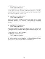
(6-7) Decrypt IC reset
Write into register
→
Resetting hardware
→
Read from register
Error
02: Reset error
05: Write data and read data do not agree.
The test is performed in the way that, after writing “0xfc” to the interrupt mask register, the registered is check if it is initialized to
“0x00” by the reset pulse signal. In addition to it, the read-data agreement check is performed for confirmation before reset.
(6-8) Decrypt IC interrupt line
ROM
→
ARP
→
Decrypt
Error
22: Decrypt interrupt is not detected.
The AC-3 audio data that is stored in ROM is transferred through ARP, and the reserve data interrupt from Decrypt is detected. Because
interrupt from Decrypt is supplied using the same interrupt line, the interrupts from Decrypt are all masked in order to identify these
interrupts.
(6-9) Reserve data top byte read
ROM
→
ARP
→
Decrypt Reserve data top byte read agreement check
Error
05: Write data and read data do not agree.
22: Decrypt interrupt is not detected.
The AC-3 audio data that is stored in ROM is transferred through ARP, and the top byte of the reserve data is read from the Decrypt
register. In the lower 4 bits at the top of the reserve data of the first 5 sectors of this audio data, the data of ‘0’, ’1’, ’2’, ’3’, ’4’ has already
been written for this check. This data is checked if the read-out data agree with this data at every interrupt into the respective sectors.
If write data and read data do not agree., check can be repeated.
(7) AV decoder
(7-2) 64020/64021 register
Write into register
→
Read from register and check if data agree
Error
05: Write data and read data do not agree.
The 51 registers that can write and read data in all bits are tested using the value of “0x00” to “0xff” with the “Data write-then-read
agreement check”. If write data and read data do not agree., check can be repeated.
(7-3) 64020/64021 reset line
Write into register
→
Resetting hardware
→
Read from register
Error
02: Reset error
05: Write data and read data do not agree.
The Capture/Compare microprocessor control register is tested by writing “0xff” into its register 0 and checks if the register is initialized
to “0xff” by the reset pulse. In addition to it, the read-data agreement check is performed for confirmation before reset.
(7-4) 64020/64021 DREQ signal line
AVD DMA check
Error
03: Data write error
04: Data read error
05: Write data and read data do not agree.
06: DMA transfer DREQ error
07: DMA transfer address error
Connection of the DREQ signal line is check by the DMA transfer with the AV decoder. When error is not detected§the transferred data
and the DRAM data that is read from the register are compared.
Summary of Contents for DVP-M35
Page 9: ...1 1 DVP M35 SECTION 1 GENERAL This section is extracted from instruction manual ...
Page 10: ...1 2 ...
Page 11: ...1 3 ...
Page 12: ...1 4 ...
Page 13: ...1 5 ...
Page 14: ...1 6 ...
Page 15: ...1 7 ...
Page 16: ...1 8 ...
Page 17: ...1 9 ...
Page 18: ...1 10 ...
Page 19: ...1 11E ...
Page 32: ......
Page 34: ......
Page 43: ......
Page 45: ......
Page 46: ......
Page 48: ......
Page 50: ......


