background image

6-10

6-6.

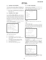
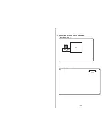
MECHA  AGING

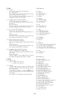
### Mecha Aging ###

Press OPEN key

Abort: STOP key

On the Test Mode Menu screen, selecting 

[3]

 executes the aging

of mechanism. First, open the tray and load a disc. Press the 

[PLAY]

key, and the aging will start. When the tray is closed, the disc type
and size are judged and displayed. During aging, the repeat cycle
is displayed. Aging can be aborted at any time by pressing the

[STOP]

 key. After the operation has stopped, unload the disc and

press again the 

[STOP]

 key or the 

[RETURN]

 key to return to the

Test Mode Menu.

6-7.

EMERGENCY  HISTORY

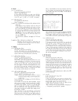
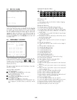
### MEG. History ###

Laser Hours

CD

xxxxxxxh

DVD

xxxxxxxh

1. 00 00 00 00

00 00 00 00

   00 00 00 00

00 00 00 00

2. 00 00 00 00

00 00 00 00

   00 00 00 00

00 00 00 00

Select: 1 – 9

Scroll: UP/DOWN

(1: Last EMG.)

Exit: Return

On the Test Mode Menu screen, selecting 

[4]

 displays the infor-

mation such as servo emergency history. The history information
from last 1 up to 10 can be scrolled with 

key or

key. Also,

specific information can be displayed by directly entering that
number with ten keys.

The upper two lines display the laser ON total hours. Data below
minutes are omitted.

Clearing History Information

Clearing laser hours
Press 

[DISPLAY]

 and 

[CLEAR]

 keys in this order.

Both CD and DVD data are cleared.
Clearing emergency history
Press 

[TITLE]

 and 

[CLEAR]

 keys in this order.

Initializing set up data
Press 

[DVD]

 and 

[CLEAR]

 keys in this order.

The data have been initialized when “Set Up Initialized” mes-
sage is displayed. The EMG. History screen will be restored
soon.

1.

3

1

2

2

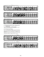
How to see Emergency History

1

: Emergency Code

2

: Don't Care

These codes are used for verification of software designing.

3

: Historical order 1 to 9

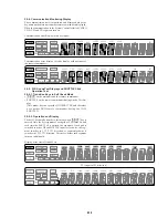
Emergency Codes List

10: Communication to IC202 (MB-101 board) failed.
11: Each servo for focus, tracking, and spindle is unlocked.
12: Communication to EEPROM, IC101 (MB-101 board) failed.
13: Writing of hours meter data to EEPROM, IC101 (MB-101

board)  failed.

14: Communication to Servo DSP IC302 (MB-101 board) failed,

or Servo DSP is faulty.

20: Initialization of tilt servo and sled servo failed. They are not

placed in the initial position.

21: Tilt servo operation error
22: Syscon made a request to move the tilt servo to wrong posi-

tion.

23: Sled servo operation error
24: Syscon made a request to move the sled servo to wrong posi-

tion.

30: Tracking balance adjustment error
31: Tracking gain adjustment error
32: Focus balance adjustment error
33: Focus bias adjustment error
34: Focus gain adjustment error
35: Tilt servo adjustment error
36: RF equalizer adjustment error
37: RF group delay adjustment error
38: Jitter value after adaptive servo operation is too large.
40: Focus servo does not operate.
41: With a dual layer (DL) disc, focus jump failed.
50: CLV (spindle) servo does not operate.
51: Spindle does not stop.
60: With a DVD disc, Syscon made a request to seek nonexistent

address.

61: With a CD disc, Syscon made a request to seek nonexistent

address.

62: With a CD disc, Syscon made a request to seek nonexistent

track No. and index No.

63: With a DVD disc, seeking of target address failed.
64: With a CD disc, seeking of target address failed.
65: With a CD disc, seeking of target index failed.
70: With a DVD disc, physical information data could not be read.
71: With a CD disc, TOC data could not be read.
80: Disc type judgment failed.
81: As disc type judgment failed, retry was repeated.
82: As disc type judgment failed, a measurement error occurred.
83: Disc type could not be judged within the specified time.
84: Illegal command code was received from Syscon.
85: Illegal command was received from Syscon.

Summary of Contents for DVP-NS900V - Sacd/dvd Player

Page 1: ...kg Operating temperature 5 C to 35 C Operating humidity 25 to 80 Supplied accessories Specifications and design are subject to change without notice Jack name Jack type Output level Load impedance AUDIO OUT L R Phono jack 2 Vrms at 50 kilohms Over 10 kilohms DIGITAL OUT OPTICAL Optical output jack 18 dBm Wave length 660 nm DIGITAL OUT COAXIAL Phono jack 0 5 Vp p 75 ohms terminated 5 1CH OUTPUT Pho...

Page 2: ...t can be measured by any one of three methods 1 A commercial leakage tester such as the Simpson 229 or RCA WT 540A Follow the manufacturers instructions to use these instruments 2 A battery operated AC milliammeter The Data Precision 245 digital multimeter is suitable for this job 3 Measuring the voltage drop across a resistor by means of a VOM or battery operated AC voltmeter The limit indica tio...

Page 3: ... DAC Schematic Diagram 4 29 MB 101 H3GA Schematic Diagram 4 31 MB 101 SACD DECODER Schematic Diagram 4 33 MB 101 DSD DSP Schematic Diagram 4 35 MS 81 LOADING Printed Wiring Board and Schematic Diagram 4 37 FR 182 Printed Wiring Board 4 39 FR 182 FUNCTION SWITCH Schematic Diagram 4 41 AU 230 Printed Wiring Board 4 43 AU 230 AUDIO Schematic Diagram 4 45 AU 230 DIGITAL OUT COAXIAL Schematic Diagram 4...

Page 4: ...REPAIR PARTS LIST 8 1 Exploded Views 8 1 8 1 1 Main Assembly 8 1 8 1 2 Chassis Assembly 8 3 8 1 3 Mechanism Deck Assembly 8 5 8 2 Electrical Parts List 8 6 Abbreviation CND Canadian HK Hong Kong KR Korea MX Mexican RUS Russian ...

Page 5: ...ptical Pick Up Page 2 4 Front Sub Panel Block Page 2 2 Power Block Page 2 3 FL 125 Board Page 2 1 FR 182 Board Page 2 2 HP 134 Board Page 2 2 Mechanism Deck Page 2 4 Tray Panel Assy Page 2 1 MB 101 Board Page 2 3 AU 230 Board Page 2 3 RY 13 Board Page 2 3 Front Panel Block Assy Page 2 1 VP 57 Board Page 2 4 EV 14 Board Page 2 4 ...

Page 6: ...Remove the top case from the set Refer to 2 1 2 Remove the MB 101 board as shown in Fig 2 4 Set the MB 101 board as shown in Fig 4 3 Set the service jig two flexible flat cables J 6090 109 A as shown in Fig 3 Fig 2 Fig 3 Fig 4 1 Flexible flat cable FMA 003 FMA 004 CN601 1 Flexible flat cable FIM 001 FIM 002 CN101 2 Connector CN101 3 Two screws B3 3 Two screws B3 4 Harness 5 MB 101 board 2 Connecto...

Page 7: ...ation and other rights owners Use of this copyright protection technology must be authorized by Macrovision Corporation and is intended for home and other limited viewing uses only unless otherwise authorized by Macrovision Corporation Reverse engineering or disassembly is prohibited Notes about the Discs On handling discs To keep the disc clean handle the disc by its edge Do not touch the surface...

Page 8: ...e player will respond to the selected command as long as the command remains in the LCD screen Some commands require you to press down on the scroll key repeatedly For a description of each command listed above refer to the pages in parentheses LCD contents Operating the LCD and scroll key Scroll key LCD screen TIME TEXT page 55 Y AUDIO page 58 Y SUBTITLE page 65 Y ANGLE page 64 Y SURROUND page 60...

Page 9: ... The VIDEO EQUALIZER indicator lights up in green when any setting other than STANDARD is selected The VIEWER indicator lights up in green when a bookmark is set Control Menu display 1 m Control Menu display 2 m ADVANCED display Appears if you select any setting other than OFF See page 57 m Control Menu display off t 16 Getting Started Quick Overview A quick overview presented in this chapter will...

Page 10: ...x To take out the disc Press A To turn off the player Press 1 on the remote The player is set to standby mode and the power indicator lights up in red Press POWER on the player to turn off completely With the playback side facing down 20 Hookups Hooking Up the Player Follow Steps 1 to 4 to hook up and adjust the settings of the player Before you start turn off the power check that you have all of ...

Page 11: ... and R rear L and R 6 speakers front L and R center rear L and R subwoofer page 25 AV amplifier receiver having a Dolby Digital or DTS decoder and a digital input jack 6 speakers front L and R center rear L and R subwoofer page 27 Stereo amplifier receiver having L and R audio input jacks only or having a digital input jack 2 speakers front L and R page 27 MD deck DAT deck page 29 AV amplifier rec...

Page 12: ...m the digital jack Connecting to a stereo amplifier receiver and 2 speakers Connecting to an MD deck or DAT deck C C 1 C 2 C 2 C 1 C 1 continued 28 C 2 C 1 SACD DVD player or Stereo amplifier receiver MD deck DAT deck Front L Front R Speakers white red red white Coaxial digital cord not supplied Stereoaudio cord not supplied to audio input to coaxial or optical digital input Optical digital cord n...

Page 13: ...r selecting the type of video signal appears 9 Press X x to select the item Select PROGRESSIVE only if you have made video connection C page 20 and wish to view progressive video signals q Press ENTER The Setup Display for selecting the type of jack used to connect your amplifier receiver appears TV Type You select Page 4 3 standard TV 4 3 LETTER BOX or 4 3 PAN SCAN 82 A wide screen TV or a 4 3 st...

Page 14: ...iver that conforms to 96 kHz digital audio input page 89 Enjoying the surround sound effects Item You select Page DISTANCE BALANCE LEVEL Set according to the connected speakers 91 Item You select Page DOWNMIX DOLBY SURROUND 88 DIGITAL OUT ON 88 SPEAKER SETUP SIZE DISTANCE BALANCE LEVEL OFF TEST TONE FRONT CENTER LARGE LARGE REAR SUBWOOFER To set press then To quit press ENTER ENTER SETUP DISPLAY D...

Page 15: ... Menu A DVD is divided into long sections of a picture or a music feature called titles When you play a DVD which contains several titles you can select the title you want using the TOP MENU button When you play DVDs that allow you to select items such as the language for the subtitles and the language for the sound select these items using the MENU button 1 Press TOP MENU or MENU The disc s menu ...

Page 16: ...e title or track in this case 01 5 Select the title chapter or track you want to program xWhen playing a DVD VIDEO For example select chapter 03 of title 02 Press X x or the number buttons to select 02 under T then press ENTER Next press X x or the number buttons to select 03 under C then press ENTER xWhen playing a VIDEO CD SACD or CD For example select track 02 Press X x or the number buttons to...

Page 17: ...orize lyrics etc 1 Press DISPLAY twice during playback when playing an SACD CD press once The Control Menu appears 2 Press X x to select A B REPEAT then press ENTER The options for A B REPEAT appear Repeating a specific portion A B Repeat Play ENTER X x DISPLAY CLEAR Scroll key SET OFF OFF 1 8 3 4 1 2 2 7 T 1 3 2 5 5 DVD VIDEO PLAY continued 48 3 Press X x to select SET t then press ENTER The A B ...

Page 18: ... disc You cannot search for a still picture on a DVD RW in VR mode 1 8 3 4 1 2 2 7 T 1 3 2 5 5 DVD VIDEO PLAY Selected row 1 2 2 7 T 1 3 2 5 5 DVD VIDEO 3 4 PLAY 52 Searching by Scene VIEWER You can divide the screen into 9 subscreens and find the desired scene quickly 1 Press DISPLAY twice during playback The Control Menu appears 2 Press X x to select VIEWER then press ENTER The options for VIEWE...

Page 19: ...ge depend on the disc you are playing xWhen playing a DVD VIDEO or DVD RW T Playing time of the current title T Remaining time of the current title C Playing time of the current chapter C Remaining time of the current chapter xWhen playing a VIDEO CD with PBC functions Playing time of the current scene xWhen playing a VIDEO CD without PBC functions SACD or CD T Playing time of the current track T ...

Page 20: ... LFE Low Frequency Effect component 1 Rear component 2 Front component 2 Center component 1 continued 60 The display examples are as follows PCM stereo Dolby Surround Dolby Digital 5 1ch When an LFE signal component is output LFE is enclosed in a solid line When an LFE signal component is not output LFE is enclosed in a broken line DTS When an LFE signal component is output LFE is enclosed in a so...

Page 21: ...d at an equal distance from your speakers and that the speakers are located in similar surroundings Otherwise the TVS effect may be hard to discern TVS NIGHT only works with Dolby Digital discs However not all discs will respond to the TVS NIGHT function in the same way If you use the DIGITAL OUT OPTICAL or COAXIAL jack and set DOLBY DIGITAL to DOLBY DIGITAL DTS to DTS in AUDIO SETUP sound will co...

Page 22: ...areas Gamma Correction below To turn off the Video Equalizer display Press O RETURN z To reset the picture items to the default values press c after Step 3 to select RESET and press ENTER z When PLAYBACK MEMORY in CUSTOM SETUP is set to ON the player will save a single setting for up to 200 individual discs This does not apply to DVD RWs in VR mode Depending on your TV or viewing environment image...

Page 23: ...e character press ENTER To overwrite do not press ENTER but move the cursor by pressing or To check the Disc Memo Toggle the scroll key up or down to display TIME TEXT in the LCD screen on the remote Then press down on the scroll key repeatedly until the Disc Memo appears at the bottom of the screen Notes During playback do not turn off the player by pressing POWER on the player Doing so may cance...

Page 24: ...play DVD VIDEOs which do not have the Parental Control function playback cannot be limited on this player Depending on the DVD VIDEO you may be asked to change the parental control level while playing the disc In this case enter your password then change the level If the Resume Play mode is canceled the level returns to the original level PARENTAL CONTROL LEVEL OFF USA STANDARD USA OTHERS PARENTAL...

Page 25: ...85 86 Kenwood 92 93 Onkyo 81 82 83 Pioneer 99 Sansui 87 Technics 97 98 Yamaha 94 95 96 80 Settings and Adjustments Using the Setup Display By using the Setup Display you can make various adjustments to items such as picture and sound You can also set a language for the subtitles and the Setup Display among other things For details on each Setup Display item see page 81 For an overall list of Setup...

Page 26: ...at is able to accept the video signal in progressive format 480p xMODE Conversion Modes DVD software can be divided into two types film based software and video based software Video based software is derived from TV such as dramas and sit coms and displays images at 30 frames 60 fields per second Film based software is derived from film and displays images at 24 frames per second In order for thes...

Page 27: ...ation If the playback sound is distorted set this item to ON The player reduces the audio output level This function affects the output of the following jacks AUDIO OUT L R 1 2 jacks 5 1CH OUTPUT jacks PHONES jack xAUDIODRC DynamicRangeControl DVD VIDEO DVD RW only Makes the sound clear when the volume is turned down when playing a DVD that has the AUDIO DRC function This affects the output from t...

Page 28: ...for the subwoofer is fixed at 120 Hz If your speakers are too small to reproduce low bass frequencies please set all speaker settings to SMALL and utilize a subwoofer for low frequency sound Even if there are fewer than 6 speakers connected the player distributes the audio signal components to the front speakers xDISTANCE You can set distance from the listening position to your speakers Set the di...

Page 29: ...ng stop press x on the player or the remote and then start playback page 39 Depending upon the disc the menu may automatically appear on the TV screen The player starts playing the disc automatically The disc features an auto playback function AUTO PLAY in CUSTOM SETUP is set to TIMER page 86 Playback stops automatically Some discs may contain an auto pause signal While playing such a disc the pla...

Page 30: ...led scenes Super Audio CD SACD page 6 An SACD disc can reproduce sounds that are extremely faithful to the original sound by use of DSD Direct Stream Digital technology This technology utilizes a sampling frequency of 2 8224 MHz which is 64 times that of a conventional CD and 1 bit quantization that enables the disc to hold 4 times the amount of information that a standard PCM format CD can hold S...

Page 31: ...MER DEMO1 DEMO2 DIMMER BRIGHT DARK AUTO DARK AUTO OFF OFF PAUSE MODE AUTO FRAME PLAYBACK MEMORY ON OFF TRACK SELECTION OFF AUTO BOOKMARK RESET t CD DIRECT OFF ON Additional Information 105 AUDIO SETUP page 88 AUDIO ATT OFF ON AUDIO DRC STANDARD TV MODE WIDE RANGE AUDIO FILTER SHARP SLOW DOWNMIX DOLBY SURROUND NORMAL DIGITAL OUT ON DOLBY DIGITAL D PCM DOLBY DIGITAL DTS D PCM DTS 48 kHz 96 kHz PCM 4...

Page 32: ...B3 1 Two tapping screws 2 Pull the tray panel assy in the direction of arrow B 3 Two claws 4 Tray panel assy 1 Insert a tapering driver into the aperture of the unit bottom and move the lever of chuck cam in the direction of arrow A B A 1 Two screws B3 6 Flexible flat cable CN802 2 Claw 7 Front panle block assy 3 Two claws 4 Claw 5 4 Flexible flat cable FLI 001 FLI 002 CN701 1 Flexible flat cable ...

Page 33: ...3 1 Connector CN501 9 HP 134 board 5 Mount HP 8 Plate HP 6 Volume knob 7 Hexagon nut M9 4 5 IF 87 board 1 Flexible flat cable FLI 001 FLI 002 CN403 3 Connector CN201 2 Two connectors CN405 452 4 Two screws B3 2 Two connectors CN406 409 1 Flexible flat cable FIM 001 FIM 002 CN407 6 Screw B3 7 Front sub panel block 1 Flexible flat cable FLI 001 FLI 002 CN403 2 Connector CN501 5 Screw B3 3 Screw B3 4...

Page 34: ...Screw B3 1 Two flexible flat cables CN203 204 3 Harness 2 Four screws B3 1 Flexible flat cable FMA 003 FMA 004 CN601 1 Flexible flat cable FMV 001 FME 002 CN502 4 MB 101 board 5 Claw 4 Six screws B3 6 AU 230 board 2 Connector CN251 3 Screw B3 1 Flexible flat cable FMA 003 FMA 004 CN101 2 Two connectors CN301 351 4 Connector CN604 6 RY 13 board 2 Two screws B3 3 Power transformer block 2 Two screws...

Page 35: ...tor 2 Insulator 1 Insulator screw 1 Insulator screw 3 Optical pick up 1 Insulator screw 2 15 MECHANISM DECK REMOVAL 4 Four screws B3 3 Screw B3 1 Flexible flat cable CN101 2 Connector CN102 5 VP 57 board 4 Eight screws B3 1 Flexible flat cable CN101 5 EV 14 board 2 Two connectors CN102 201 3 Two screws B3 1 Three screws B3 2 Mechanism deck ...

Page 36: ...2 5 2 17 INTERNAL VIEWS Optical pick up KHM 240AAA J1RP 8 820 144 06 DC motor loading not supplied DC motor loading not supplied ...

Page 37: ... MB 101 SIGNAL PROCESS SERVO AU 230 AUDIO DIGITAL OUT COAXIAL VP 57 VIDEO Except AEP UK Russian EV 14 VIDEO AEP UK Russian RY 13 RELAY Power Block HS15S1E EXCEPT US Canadian Mexican Power Block HS15S1U US Canadian Mexican FL 125 IF CON IF 87 INTERFACE CONTROL HP 134 HEAD PHONE ...

Page 38: ... VIDEO OUT S VIDEO OUT 5 1CH OUTPUT CENTER WOOFER FRONT REAR L R L R L R L R OPTICAL DIGITAL OUT COAXIAL J351 IC201 VIDEO BUFFER SELECT SW RY201 203 206 SW IC105 VIDEO BUFFER IC107 VIDEO BUFFER IC106 IC102 J301 J302 J303 VP 57 BOARD SEE PAGE 4 63 to 4 72 VIDEO BUFFER INTERLACE IC101 GATE ARRAY IC203 16M SDRAM Y Cb Cr Y Cb Cr Y Cb Cr Y0 7 CB0 7 CR0 7 COMPONENT VIDEO OUT 2 1 S VIDEO OUT VIDEO BUFFER...

Page 39: ...LIMIT SENSOR TRACKING COIL FOCUS COIL M001 LOADING MOTOR M M M M M M MS 81 BOARD SEE PAGE 4 38 SLED MOTOR SPINDLE MOTOR CN204 39 VCI 19 39 20 22 16 17 168 GIO2 INT4 05 CHUCK TRAY DETECT S001 1 2 RF A D E H VC PD 24 10 LDSEL0 SW DVD LD 26 6 Q202 CD LD DRIVE CDLD CD LD VR SLA SLB SPM INLIM TRK 139 ADC3 FCS PS TSD M 40 42 43 VREF 3 3V LDON 173 ı 175 180 GIO6 SDI GIO7 SDO GIO8 SCK GIO13 XSDPIT XSDPCS ...

Page 40: ...CAS RAS OE WE RAS LCAS UCAS PDO 0 7 PDO 0 7 PDI 0 7 PDI 0 7 YCIN 0 7 YCOUT 0 7 VIDEO 1 SEE PAGE 3 9 AUDIO 1 SEE PAGE 3 15 AUDIO 1 SEE PAGE 3 15 27MVGA32 MRST CK27 NRSDIN SCS FID H SYNC NRSDOUT NRSENB VREFI D1CLKO ACH12 ACH34 FLDO HSYNCO ACH56 LRCKO BCKO ACH12 ACH34 ACH56 LRCK BCK VIDEO LEVEL ADJ RV501 XRST HD 0 15 HAD 0 21 HA 0 21 HD 0 15 D 0 7 A 0 7 CDDOUT HA 0 7 HD 8 15 XRD XWRH RSTB DM ACK1 DM ...

Page 41: ...UTE 21 X38IT INT5 22 CMDREQ INT6 40 DVD SACD DVD SACD 8 XSACS XSACS 78 XBMCS XBMCS XARPRST INT1 CS4X XWAIT 35 XRST XRST XRST XRD XWRH XWRL 512 2OUT 3 512FS38 27 1OUT 4 27M38 27 2OUT 15 33 1OUT 13 33MSA 33 2OUT 512 1OUT XTI XTO 27MAVD X1 X2 HD 0 15 HA 0 21 XRD XWRH XRD XWRH XRD XWRH XGAWT 2 CN101 6 5 7 4 3 16 WP SCL SDA 77 59 65 89 86 85 CPUCK XRAMCS XGACS OCSW1 TSW2 SCL SDA WP 41 37 42 RBGSEL DISC...

Page 42: ...EVEL RV101 34 S LEVEL RV102 1 ı 8 8 20 40 31 30 38 DCLK 128 RV301 16 ı 23 42 ı 49 4 ı 11 125 132 ı 137 139 25 PHSYNC 129 29 PVSYNC 130 28 PBLANK 131 27 2 1 16 15 12 5V SCAN SELECT S301 PROGRESSIVE INTERLACE SELECTABLE 3 ı 10 CLKIN RSET1 RESET B SCL SDA RSET2 P0 7 RESET B SDA SCL CLKIN V2 9 U2 9 Y2 9 CR0 7 CB0 7 Y0 7 HSYNC VSYNC BLANK CLKOUT RESET CLK27M SCL SDA SCL SDA SCL SDA CN101 IPSW EUROVY DV...

Page 43: ...SEE PAGE 4 69 70 71 72 VIDEO OUT S VIDEO OUT Y C Y C 11 15 13 7 1 4 Q308 309 WIDE SWITCH DRIVE IC306 VIDEO BUFFER VIDEO 1 SEE PAGE 3 9 VIDEO OUT S Y S C VIDEO 1 SEE PAGE 3 9 MUTE1 MUTE2 V IN Y IN C IN V OUT Y OUT C OUT 5 DSEL VMUTE WIDE CN102 8 05 VIDEO 1 SEE PAGE 3 9 INTERFACE CONTROL SEE PAGE 3 19 Q312 WIDE SWITCH Q311 WIDE SWITCH 2 2 Vp p H IC306 qg 1 5 Vp p H IC307 2 1 8 Vp p H IC306 qd 2 4 Vp...

Page 44: ... V_IN V_OUT BLANKING IN R_IN G_IN AVLINKI FUNCTION_SW_IN B_IN A L IN A L OUT A R IN A R OUT V_IN V Y_OUT BLANKING OUT R C_OUT G_OUT AVLINKO FUNCTION_SW_OUT B_OUT A L IN A L OUT A R IN A R OUT CN203 CN202 LINE 1 RGB TV LINE 2 Y J101 J102 VIDEO OUT PB PR S VIDEO OUT J103 CN102 CN201 RV101 48 RSET1 30 SCL 31 SDA 49 RESET B 27 CLKIN 34 RSET2 44 DAC B 41 DAC C 40 DAC D 36 DAC F 37 DAC E IC102 VIDEO D A...

Page 45: ...4 DSP2DIACKI 67 DSP2ACKI 8 DSP1DIACKI D603 D602 D601 3 5 6 7 1 2 6 MADATO 4 MSDATI SI1 SO1 SC1 3 MSCK 4 MSDATO 5 MSDATI SI1 SO1 SC1 6 MSCK 123 A 0 11 DQ 0 7 131 134 136 139 148 149 151 152 154 157 159 162 IC803 16M SDRAM IC806 SACD DECODER IC804 BUFFER SDI 0 7 WSAD 0 7 WCK XSHD SDCK XSAK SDEF A 0 11 WAD 0 7 SD 0 7 DQ 0 7 DCLK DCKE XWES XCAS XRAS 2 B 4 Y 66 69 71 74 DSAR DSAC DSALFE DSALS 76 DSARR ...

Page 46: ...2 1 7 3 5 IC251 HEADPHONE AMP D251 TIMING Q252 MUTE Q251 MUTE D352 SURGE PROTECT 1 2 HP 134 BOARD SEE PAGE 4 50 RV501 LEVEL J501 PHONES J352 S LINK CN201 AUDIO OUT2 R L R L AUDIO OUT1 R L WOOFER CENTER R L 5 1CH OUTPUT R L FRONT REAR IC352 OPTICAL DIGITAL OUT 1 D IN COAXIAL J351 J101 Q351 BUFFER AU 230 BOARD SEE PAGE 4 45 to 4 48 CN101 10 8 12 14 3 5 4 6 11 13 9 7 MUTE_L MUTE_R MUTE_23 16 18 19 24...

Page 47: ..._CW ENTER RIGHT UP LEFT DOWN x S809 FR 182 BOARD SEE PAGE 4 41 FL 125 BOARD SEE PAGE 4 57 S_LINK IFRST 7 27 14 16 15 17 23 24 FRRST BUSY CS SO SI SC AMUTE VMUTE 2 XIN 3 XOUT 33 AD3 11 IR 21 BUZ 25 STATUS 43 LED_PLAY 42 LED_PAUSE 22 JOG_LED 31 AD1 34 AD4 35 AD5 36 AD6 18 JOGCW 12 JOG_CCW 37 CURSOR 8 RST 45 LED_MULTII 41 LED_SACD 44 LED_DVD 79 LED_FLOFF 80 LED_VOFF 05 CN701 BZ701 BUZZER IF 87 BOARD ...

Page 48: ... 3 23 EVER 3 3V SW 5V SW 3 3V 1 8V 3 3V MNT PCONT 3 3V_MNT M 11V DOWNLOAD POWER 2 SEE PAGE 3 23 ACOUTN ACOUTL CN606 1 3 CN601 LF601 LINE FILTER RY601 3 4 1 2 1 CN603 3 CN604 T901 POWER TRANS ACOUT L ACOUT N AC_10V AC_10V POWER 2 SEE PAGE 3 23 RY 13 BOARD SEE PAGE 4 74 FILTER 2 4 1 SW 5V SW 11V 11V AUDIO CN102 FL107 FILTER FL108 FILTER FL109 IC301 5V REG 3 OUT 1 IN 2 SW IC104 3 3V REG 3 OUT 1 IN IC...

Page 49: ... FLASH IC107 OTP FILTER FL105 or IC801 2 5V REG 4 VOUT 5 VIN IC806 SACD DECODER FILTER FL801 FILTER FL803 1 2 20 21 POWER 1 SEE PAGE 3 21 8 05 1 4 CN301 AC_10V AC_10V 20 21 D301 D302 D303 D304 IC301 1 2 Q302 303 12V REG IC301 2 2 Q301 12V REG IC251 5 1CH CENTER WOOFER AUDIO AMP IC103 5 1CH REAR AUDIO AMP IC101 AUDIO AMP IC102 5 1CH FRONT AUDIO AMP IC352 OPTICAL DIGITAL OUT IC351 5V REG 3 OUT 1 IN ...

Page 50: ...ammable resistor 5 fusible resistor C panel designation f internal component C adjustment for repair U B Line V B Line Circled numbers refer to waveforms Voltages are dc between measurement point Readings are taken with a color bar signal on DVD refer ence disc and when playing CD reference disc Readings are taken with a digital multimeter DC 10MΩ Voltage variations may be noted due to normal prod...

Page 51: ...11V EVER 11V D_GND P CONT 11V AUDIO SW 11V SW 3 3V P DET M_GND ACOUT L NC GND ACOUT N 11V ACOUT N ACIN N ACIN L NC ACOUT L HARNESS GND S_LINK A_MUTE EVER 3 3V FFC SPM GND GND GND INLIM N C TRK DVD LD LED N C PD SLA VC SLB FCS B VCC C FCS F SLB E TRK MOD RF SW N C D VR G SPM H CD LD N C LD GND SLA A ROUT3 MUTE_L P_GND_2CH P_GND_6CH MUTE_23 LOUT1 ROUT2 P_GND_6CH LOUT2 ALT ALT LOUT2 A 5V P_GND_2CH RO...

Page 52: ... 3 3V TXD GND RXD GND RF MON GND DVD 3 SCL DVD 6 27MCLK GND DVD 2 DVD 7 XRST WIDE DVD 1 DVD 5 SDA DVD 0 DVD 4 IPSW EUROVY FMV 001 IV 056 FLR 002 FLR 003 GND V_MUTE SW 5V 11V AUDIO SW 11V GND A_MUTE FLI 001 EXCEPT AEP UK RUS GND EVER 11V IFRST SI0 SW 5V SO0 SW 5V P DET P CONT GND P DET V_MUTE GND S_LINK EVER 11V SI0 SW 11V SO0 GND IFRST FFC XIFCS SW 11V IFBSY 3 3VMNT SW 11V IFRST SC0 V_MUTE IFBSY 3...

Page 53: ...503 A 1 IC601 D 2 IC602 D 1 IC806 D 4 RV501 B 2 4 2 PRINTED WIRING BOARDS AND SCHEMATIC DIAGRAMS MB 101 SIGNAL PROCESS SERVO PRINTED WIRING BOARD Ref No MB 101 board 2 000 series MS 81 LOADING FR 182 FUNCTION SWITCH MB 101 SIGNAL PROCESS SERVO AU 230 AUDIO DIGITAL OUT COAXIAL VP 57 VIDEO Except AEP UK Russian EV 14 VIDEO AEP UK Russian RY 13 RELAY Power Block HS15S1E EXCEPT US Canadian Mexican Pow...

Page 54: ... MB 101 MB 101 BOARD SIDE B D601 D 1 D602 D 1 D603 D 1 IC101 B 7 IC103 C 5 IC106 A 6 IC107 A 6 IC201 D 5 IC202 D 7 IC301 D 5 IC303 C 6 IC501 C 3 IC504 B 2 IC507 B 3 IC603 D 1 IC604 D 1 IC801 E 4 IC803 D 4 IC804 E 4 IC807 D 3 Q201 E 5 Q202 E 4 ...

Page 55: ...LB DVD_LD G CD_LD B H F TE E PI FE FCS A SSWD SSCK SSRD E F SSCS G TZC TRK CD_LD DVD_LD H TRK C FCS D INLIM TE FE PI SSRD SSDFCTI SSWD D C B A V33 VCI TPH LED WPP TRK H DFT VPB SLA CN TRK B TZC SWD D2 H FCS A PII SCLK D SLB G SLB F BYP2 LDSELO MON C2 INLIM VCC ATON LDON FE RFIP SLA GND RF MIRR MEVO DVDPD SPM MOD FNN MP CDPD A2 SPM VC ATOP DVDLD VNB B VR FNP VC C GND GND BYP PI SRD E N C RX C TE AI...

Page 56: ...34 35 41 42 43 44 45 46 11 15 36 40 24 25 47 48 49 50 JL312 4700 R346 0 R322 2700 R335 0 01u C342 2200 R333 4700p C308 0 01u C315 JL339 0 01u C323 3300 R306 JL327 JL336 33k R325 0 01u C325 4700 R345 0 1u C310 0 033u C311 6 3V 100u C302 MM1385ENLE IC301 1 2 3 4 5 0 01u C348 SS_MON 0 R356 1 A TCK MEMD3 MEMD4 MEMD2 MEMD7 MEMD0 MEMD5 MEMD1 TMS TRST MEMA9 MEMA1 TDOGA TDOKT MEMD6 MEMA0 MEMD13 MEMA2 MEMA...

Page 57: ...82 AVSS_06 183 AVDD_07 184 VC 185 CPOT 186 AVDD_08 187 N C BUS_CLOCK 188 IOVDD_12 189 HAD23 190 HAD22 191 HAD21 192 HAD20 193 CVS09 194 HAD19 195 HAD18 196 HAD17 197 HAD16 198 IOVSS_12 199 HAD15 200 HAD14 201 HAD13 202 HAD12 203 CVD09 204 HAD11 205 HAD10 206 HAD9 207 HAD8 208 IOVDD_13 209 HAD7 210 HAD6 211 HAD5 212 HAD4 213 CVS10 214 HAD3 215 HAD2 216 HAD1 217 HAD0 218 IOVSS_13 219 HCSB 220 HRWB 2...

Page 58: ... ADDT11 ADDT3 ADAD0 ADDT1 ADAD3 ADAD5 ADDT8 ADAD5 ADDT12 ADAD0 ADDT10 ADAD9 ADAD7 ADDT12 ADAD2 ADAD4 ADAD3 ADAD4 ADAD10 ADDT5 ADAD1 ADDT7 ADDT6 ADDT9 ADAD8 ADDT4 ADDT5 ADDT13 ADAD11 ADDT15 ADDT15 ADDT3 ADDT7 ADAD7 ADAD10 ADDT0 ADAD8 ADDT1 ADAD9 ADDT14 ADDT8 ADDT4 ADDT13 ADDT10 ADDT0 ADDT9 ADDT11 PDI5 PDI2 PDI1 PDI0 PDI7 PDI6 PDI3 PDI4 PDO5 PDO4 PDO3 PDO2 PDO1 PDO0 PDO7 ADAD3 ADAD2 ADAD1 ADAD0 ADAD...

Page 59: ...46 150k R221 33k R240 10k R229 470k R233 JL205 120k R218 4700p C230 0 001u C228 33k R252 10k R274 22k R275 10k R276 0 R271 FAN8034 IC202 1 2 3 4 5 6 14 15 16 17 18 19 20 21 22 23 24 27 28 29 30 31 32 33 34 35 36 40 41 42 43 44 45 46 47 48 50 51 52 49 13 25 26 37 38 39 11 12 9 10 7 8 1 A 3 2 1 5P CN201 1 2 3 4 5 SPM LDM LDM SPM CKSW1 OCSW1 OCSW1 CKSW1 LDM LDM SLB SLA SLA SLB FCS TRK TRK INLIM FCS O...

Page 60: ...5 GND 12k R154 YUVRGB RGBSEL EUROVY DISCEXT SDA SCL IP_SW 3300 R124 4 7k R173 R157 R152 SI0 HDI5 HDI4 HAI2 HAI3 HAI4 HAI1 HAI5 HAI9 HAI6 HAI8 HAI7 HAI12 HAI10 HAI11 HAI14 HAI16 HAI13 HAI15 HDI12 HDI9 HDI8 HDI10 HDI11 HDI15 HDI14 HDI13 HAI0 HAI20 HAI21 SI2 HAI19 SO0 HAI18 SC0 HAI17 SO2 HDI0 HDI1 HDI2 HDI3 HDI6 HDI7 48 44 1K SC0 X38CS A2 SI1 XDACS SO1 XBMCS SC1 CPUCK XIFCS XFRRST A0 DACK1 VSS DREQ1 ...

Page 61: ...0 GND 3 3V 17 16 5 4 1 A IMIC6001BTD IC103 1 2 3 4 5 6 7 8 9 10 11 12 13 14 15 16 SC0 SO0 SI0 SO0 VSS VDD 33 2OUT FSEL 1 8V GND GND 33 1OUT N C XTO 512 2OUT 512 1OUT GND 27M VSS 3 3V VSS SW 5V SC0 VDD 3 3V_MNT VDD XFRRST M_GND 27 2OUT IFBSY XIFCS M 11V 27 1OUT SI0 XTI M_GND M 11V 11 8 3 9 F 2 4 D 5 10 E 6 7 05 MB 101 BOARD 7 13 B C IC103 PLL CN407 SEE PAGE 4 54 IF 87 BOARD CN404 SEE PAGE 4 54 IF 8...

Page 62: ...6 HAI12 HAI17 HDI1 HDI12 HAI17 HAI1 HDI1 HAI9 HAI11 HAI20 HDI4 HDI2 HAI9 HAI3 HAI10 HDI14 HDI9 HAI18 HAI7 HDI13 HAI2 HAI0 HDI10 HAI6 HAI11 HAI5 HAI3 HAI12 HAI1 HAI21 HDI3 HAI13 HDI5 HAI16 HAI17 HAI19 HAI2 HAI5 HAI4 HDI7 HDI11 HDI8 HAI15 HAI3 HAI14 HAI6 HAI5 HDI3 HDI12 HDI4 HAI16 HDI11 HAI13 HAI16 HAI6 HDI15 HDI3 HAI2 HAI20 HAI4 HAI7 HAI13 HAI19 HDI7 HAI19 HDI7 HDI15 HDI6 HAI1 HDI9 HAI18 HDI10 HDI0...

Page 63: ...MS TRST TCK IOVDD17 GND32 CVD12 DSP1BCKI GND33 DSP1ACKI GND34 DSP1NMII GND35 DSP1REQI0 IOVDD18 GND36 CVD13 DSP1EMPI DSP1CH56I DSP1CH34I DSP1CH12I DSP1LRCKI IOVDD19 GND37 CVD14 DSP1CH78O DSP1CH56O DSP1CH34O DSP1CH12O IOVDD20 GND38 DSP1DO DSP1EMP0 DSP1BCK0 DSP1LRCK0 IOVDD21 GND39 CVD00 DSP1ACKO2 DSP1ACKO1 DSP1ACKO0 GND00 RESET_NI GND01 DSP1DIACKI NC GND02 DSP1DII IOVDD0 GND03 CVD01 PLL27_CLNI PLL_EN...

Page 64: ...1 2 3 1 A ROUT1 DZF23 DZF23 ROUT1 ART LOUT2 ART LOUT2 DZFL1 MUTE_R ROUT2 MUTE_23 ROUT2 DZFR1 DZFR1 LOUT3 LOUT3 MUTE_L ROUT3 ALT DZFL ROUT3 ALT DZFL DZFL1 LOUT1 DZFR LOUT1 ART ALT ART ALT MUTE_23 MUTE_R MUTE_L LOUT2 ROUT2 LOUT2 ROUT2 ROUT3 LOUT1 ROUT3 LOUT3 ROUT1 ROUT1 LOUT1 LOUT3 PDN DCLK PDN CAD0 ART LOUT3 LOUT2 ROUT1 ROUT3 CSN AVDD DVDD LOUT2 CCLK AOUTL DSDL3 MUTE_L LRCK DSDR P_GND_2CH P_GND_6CH...

Page 65: ...M TRMP K9F3208W0A TCB0T IC404 1 2 3 4 5 6 7 8 9 10 15 16 17 18 19 20 21 22 23 24 25 26 27 28 29 30 31 32 35 36 39 40 41 42 43 44 13 14 37 38 0 01u C427 10k R428 HD15 HA0 HA1 HA2 HA3 HA4 HA5 HA6 HA7 HA8 HA9 HA10 HA11 HA12 HA13 HA14 HA15 HD1 HD2 HD3 HD4 HD5 HD6 HD7 HD8 HD9 HD10 HD11 HD12 HD13 HD14 DSENS TSENS OCSW2 HA15 HA14 HA13 HA12 HA11 HA10 HA9 HA8 HA7 HA6 HA5 HA4 HA3 HA2 HA1 HA0 HD0 HD1 HD2 HD3...

Page 66: ...802 10k R815 JL840 JL837 0 01u C828 22 R826 JL850 JL809 0 R824 HY57V161610DTC 7TR IC803 1 VCC 2 DQ0 3 DQ1 4 VSSQ 5 DQ2 6 DQ3 7 VCCQ 8 DQ4 9 DQ5 10 VSSQ 11 DQ6 12 DQ7 13 VCCQ 14 DQML 15 WE 16 CAS 17 RAS 18 CS 19 A11 BA 20 A10 AP 21 A0 22 A1 23 A2 24 A3 25 VCC 26 VSS 27 A4 28 A5 29 A6 30 A7 31 A8 32 A9 33 N C 34 CKE 35 CLK 36 DQMU 37 N C 38 VCCQ 39 DQ8 40 DQ9 41 VSSQ 42 DQ10 43 DQ11 44 VCCQ 45 DQ12 ...

Page 67: ...JL855 0 R852 100 R864 R820 0 0 R868 0 R874 0 R871 JL872 JL875 JL862 0 01u C837 JL864 0 01u C839 6 3V 47u C836 0 R856 0 R876 JL866 0 01u C834 JL861 JL857 0 R855 0 01u C838 0 R870 JL816 JL815 0 R880 17 10 9 11 12 13 14 15 16 1 A 1 2 3 4 5 6 7 8 XBMCS SC1 SO1 SI1 XBMCS SI1 SO1 SC1 GND AMC FS128 TEST2 FS64 GND DSI1 GND DSI2 VDD DSI3 GND DSI4 GND DSI5 VDD DSI6 GND DSD1 DSD2 MUDAT BCKDSL BCKDO BCKDI GND...

Page 68: ...JL002 JL003 JL004 JL005 1 A LDM LDM OCSW1 CKSW1 GND MB 101 BOARD 5 13 CN402 SEE PAGE 4 19 LOADING MOTOR DETECT CHUCK TRAY 2 4 5 05 B MS 81 BOARD 3 C MS 81 LOADING FR 182 FUNCTION SWITCH MB 101 SIGNAL PROCESS SERVO AU 230 AUDIO DIGITAL OUT COAXIAL VP 57 VIDEO Except AEP UK Russian EV 14 VIDEO AEP UK Russian RY 13 RELAY Power Block HS15S1E EXCEPT US Canadian Mexican Power Block HS15S1U US Canadian M...

Page 69: ... mounted in this model is printed on this diagram MS 81 LOADING FR 182 FUNCTION SWITCH MB 101 SIGNAL PROCESS SERVO AU 230 AUDIO DIGITAL OUT COAXIAL VP 57 VIDEO Except AEP UK Russian EV 14 VIDEO AEP UK Russian RY 13 RELAY Power Block HS15S1E EXCEPT US Canadian Mexican Power Block HS15S1U US Canadian Mexican FL 125 IF CON IF 87 INTERFACE CONTROL HP 134 HEAD PHONE ...

Page 70: ...8 JL809 JL810 JL811 JL813 JL817 JL818 JL819 JL820 JL821 JL822 JL823 JL824 JL825 14P CN801 1 2 3 4 5 6 7 8 9 10 11 12 13 14 UN2213 TX Q801 UN2213 TX Q802 3900 R813 10k R811 22k R815 8200 R814 2700 R812 S809 S801 S803 S805 S807 S802 S804 S806 S808 S810 S811 UN2213 TX Q803 1 A GND DOWN RIGHT LEFT TO JOG COMMON JOG_CCW ENTER JOG_CW UP PLAY_LED PAUSE_LED JOG_LED GND AD1 AD4 AD5 AD6 JOG_CCW JOG_CW COMMO...

Page 71: ...IC102 C 6 IC103 C 7 IC201 C 3 IC251 C 2 IC301 C 9 IC351 B 2 IC352 A 2 Q101 B 4 Q102 B 5 Q103 B 6 Q104 B 6 Q105 B 7 Q106 B 7 Q201 B 3 Q202 B 3 Q251 D 2 Q252 C 2 Q301 C 8 Q302 C 9 Q303 D 10 Q351 B 1 Q352 D 6 Q353 D 5 Q354 D 6 Q355 D 7 Q356 D 6 Q357 D 6 Q358 D 7 Q359 D 7 Q360 D 7 MS 81 LOADING FR 182 FUNCTION SWITCH MB 101 SIGNAL PROCESS SERVO AU 230 AUDIO DIGITAL OUT COAXIAL VP 57 VIDEO Except AEP U...

Page 72: ...P Q302 10k R366 50V 1u C359 4700 R359 25V 100u C212 10k R367 JL356 Q358 UN2213 TX NJM4580E D TE2 IC301 1 2 3 4 5 6 7 8 4P CN301 1 AC_10V 2 N C 3 GND 4 AC_10V 11EQS04 TA1B D301 2400 R214 100k R226 680 R212 47k R364 2SA985A QP Q301 1k R207 C306 63V 47u 3300 R224 47k R368 680 R215 35V 1000u C305 50V 1u C360 16V 1000p C361 DAN202K T 146 D351 3300 R223 C309 63V 47u 11EQS04 TA1B D302 220 R218 C204 4700p...

Page 73: ... 3300 3300 R260 JL107 JL104 R146 2400 220 R354 33k R254 C109 4700p C134 0 1u JL101 R131 1200 GP1FA551TZ IC352 D IN 1 VCC 2 GND 3 Q104 2SD1938 F T TX SO C133 0 1u IC103 NJM2114D 1 2 3 4 5 6 7 8 JL117 R153 47k 25V C128 100u R158 47k 33k R253 R129 680 100 R257 JL102 JL113 2SC2712 YG TE85L Q351 1k R109 R118 1k C120 1200p R162 3300 R124 2400 C114 470p R135 680 1k R353 NJM4580E D TE2 IC251 1 2 3 4 5 6 7...

Page 74: ...U US Canadian Mexican FL 125 IF CON IF 87 INTERFACE CONTROL HP 134 HEAD PHONE AEP UK RUS AEP UK RUS AEP UK RUS US CND MX HR KR US CND MX HR KR AEP UK RUS 1500p C503 1500p C504 W501 JS501 JS502 JL501 HZM6 8ZWA1TL D501 JL502 HZM6 8ZWA1TL D502 FB502 0uH JL506 J501 JL503 JL504 1500p C502 FB501 0uH 1500p C501 RV501 500 500 2P CN501 1 2 1 A DIP PIN LAND HP L HP R PHONES MAX MIN LEVEL AU 230 BOARD 2 2 CN...

Page 75: ...CN401 B 11 CN402 B 10 CN403 C 13 CN404 C 3 CN405 A 10 CN406 B 4 CN407 C 1 CN408 C 2 IC401 B 5 Q401 A 10 Q402 A 10 MS 81 LOADING FR 182 FUNCTION SWITCH MB 101 SIGNAL PROCESS SERVO AU 230 AUDIO DIGITAL OUT COAXIAL VP 57 VIDEO Except AEP UK Russian EV 14 VIDEO AEP UK Russian RY 13 RELAY Power Block HS15S1E EXCEPT US Canadian Mexican Power Block HS15S1U US Canadian Mexican FL 125 IF CON IF 87 INTERFAC...

Page 76: ... R417 3W 6 8 R418 1 A XIFCS SC0 SOO SIO XIFBUSY XFRRST 3 3V_MNT GND IFRST P CONT P DET D_GND D_GND SW 3 3V EVER 3 3V 5V 11V AUDIO PCONT M_GND M_GND SW 11V SW 11V EVER 11V VOUT GND VIN 3 3V_MNT XFRRST IFBSY SI0 SO0 SC0 GND XIFCS SW 3 3V GND SW 5V GND 1 8V M_GND M 11V M 11V M_GND P DET P CONT SW 11V SW 11V EVER 11V GND EVER 3 3V GND GND SC0 SO0 SI0 XIFCS IFBSY IFRST 3 3VMNT A_MUTE V_MUTE S_LINK IFRS...

Page 77: ...rinted on this diagram FL 125 BOARD SIDE B CN701 C 10 CN702 A 7 D701 B 11 D704 C 12 D705 B 11 D706 C 4 D711 A 9 D713 A 8 D714 A 7 D715 A 10 IC701 B 12 IC702 B 11 Q702 C 11 Q703 C 11 Q707 A 8 Q708 B 7 FL 125 BOARD SIDE A D702 C 7 D703 C 8 D707 B 10 D708 B 10 D709 B 10 D710 B 10 D712 C 9 D716 C 9 IC703 B 8 IC704 B 9 Q704 B 10 Q705 B 10 Q706 B 9 Q709 A 4 Q710 A 11 Q711 A 11 ...

Page 78: ...10 UN2213 TX Q711 22k R712 21P CN701 1 2 3 4 5 6 7 8 9 10 11 12 13 14 15 16 17 18 19 20 21 10k R705 TMP86CK74F 3G50 IC703 1 2 3 4 5 6 7 8 9 10 11 12 13 14 15 16 17 18 19 20 21 22 23 24 25 26 27 28 29 30 31 32 33 34 35 36 37 38 39 40 41 42 43 44 45 46 47 48 49 50 51 52 53 54 55 56 57 58 59 60 61 62 63 64 65 66 67 68 69 70 71 72 73 74 75 76 77 78 79 80 JL735 JL733 JL734 1 A SEG10 SEG9 SEG14 SEG13 SE...

Page 79: ... 1 IC306 A 3 Q107 B 5 Q108 B 5 Q109 B 4 Q110 B 4 Q111 B 3 Q112 B 3 Q113 B 5 Q114 B 4 Q115 B 4 Q304 B 7 Q305 B 6 Q306 B 6 Q307 C 7 Q308 B 3 Q309 B 3 Q310 C 7 Q311 B 3 Q312 B 3 Q313 C 7 Q314 C 6 Q317 C 7 MS 81 LOADING FR 182 FUNCTION SWITCH MB 101 SIGNAL PROCESS SERVO AU 230 AUDIO DIGITAL OUT COAXIAL VP 57 VIDEO Except AEP UK Russian EV 14 VIDEO AEP UK Russian RY 13 RELAY Power Block HS15S1E EXCEPT ...

Page 80: ...CN101 C 2 CN102 C 5 D311 C 7 IC104 C 4 IC201 B 2 IC202 B 1 IC204 B 1 IC301 C 7 IC302 C 6 IC303 C 5 IC304 C 6 IC307 A 5 IC308 A 5 Q101 B 4 Q102 B 4 Q103 B 4 Q104 B 3 Q105 B 3 Q106 B 3 Q116 C 7 Q117 C 7 Q301 B 6 Q302 B 6 Q303 B 5 Q318 A 5 Q319 A 5 Q320 A 6 ...

Page 81: ...7 10 R126 JL194 JL186 JL503 JL112 JL114 JL506 JL183 JL175 JL188 0 001u C105 0 01u C109 JL116 10 R117 JL136 JL180 4700 R131 4700 R509 10 R105 27MCLK1 UN2111 TX Q116 1k R142 UN2213 TX Q117 VMUTE 5P CN102 1 2 3 4 5 1 2 3 GND 1 A RLO2 GBE1 GBE3 GLO3 RRO1 BLO5 BRO0 GRO7 GRE6 GBE4 Y5 GLO0 RLO1 GBE5 GRE3 BRO1 BRO4 CB2 GRE4 GGE5 GRE3 RRO1 GLO1 BRO3 GLO3 RLO5 BRO2 GLO2 GRO3 CR5 GRE7 GBE7 GRO6 RRO5 BRO1 GBE...

Page 82: ...12 YG TE85L Q101 JL514 C120 0 01u 180 R164 1k R178 0 01u C122 JL512 22 R184 0 01u C128 R139 330 C117 0 1u FL104 7 1 2 3 4 5 6 8 9 10 13 15 16 18 12 2SA1162 YG TE85L Q112 2SA1162 YG TE85L Q107 R132 10k 1k R156 1k R179 6 3V 47u C134 2SA1162 YG TE85L Q109 C110 0 01u 2SC2712 YG TE85L Q102 R138 330 180 R169 2200 R188 22 R147 0 01u C127 100 R134 0 1u C118 2200 R172 2200 R175 2200 R190 R141 330 0 01u C13...

Page 83: ...51 42 50 41 49 40 48 39 47 38 46 37 45 145 146 147 148 149 150 151 152 153 154 155 156 157 158 159 160 161 162 163 164 165 166 167 168 169 170 171 172 173 174 175 176 177 178 179 180 181 182 183 184 185 186 187 188 189 190 191 192 193 194 195 196 197 198 199 200 201 202 203 204 205 206 207 208 10 R227 0 1u C213 6 3V 47u C218 22 R258 100k R211 10 R247 100 R203 1 A GBE7 GBE6 GBE5 GBE4 GBE3 GBE2 GBE1...

Page 84: ...0 R320 0 1u C342 C331 0 1u 6 3V 47u C335 10 R302 RY301 1 8 3 2 4 6 7 5 2200 R364 10 R308 330 R349 0 001u C316 10k R379 2SC2712 YG TE85L Q303 0 01u C332 6 3V 47u C311 0 R315 10 R317 C329 0 1u 6 3V 47u C336 1k R367 FL301 7 1 2 3 4 5 6 10 12 9 1k R366 UN2111 TX Q313 680 R354 330 R348 0 1u C317 470p C321 2200 R365 10 R324 2SC2712 YG TE85L Q301 JL301 10 R301 22 R351 UN2111 TX Q317 10 R328 10k R382 0 01...

Page 85: ...655 R650 0 Q311 UN2111 TX R649 0 JL312 100uH L303 R604 10k 1k R657 R645 75 47k R374 0 01u C353 6 3V 47u C339 Y C G G C G G Y J302 2 1CGND 1 1YGND 4 1C 3 1Y 6 2CGND 5 2YGND 8 2C 7 2Y 9 S1 10 S2 JL307 6 3V 47u C343 10k R381 0 01u C354 0 1u C350 0 01u C352 UN2111 TX Q309 1k R662 0 01u C351 R652 0 D305 HZM6 8ZWA1TL 6 3V 47u C344 R653 0 HZM6 8ZWA1TL D309 6 3V 47u C338 UN2213 TX Q308 J301 1 1V 3 GND 2 2...

Page 86: ...9 2 6 7 4 C 05 B RY 13 BOARD D 5 3 4 73 4 74 RELAY RY 13 RY 13 RELAY PRINTED WIRING BOARD AND SCHEMATIC DIAGRAM Ref No RY 13 board 1 000 series There are a few cases that the part isn t mounted in this model is printed on this diagram MS 81 LOADING FR 182 FUNCTION SWITCH MB 101 SIGNAL PROCESS SERVO AU 230 AUDIO DIGITAL OUT COAXIAL VP 57 VIDEO Except AEP UK Russian EV 14 VIDEO AEP UK Russian RY 13 ...

Page 87: ...DVP NS900V 4 75 4 76 VIDEO EV 14 EV 14 VIDEO PRINTED WIRING BOARD Ref No EV 14 board 4 000 series AEP UK RUS There are a few cases that the part isn t mounted in this model is printed on this diagram ...

Page 88: ...2 3 4 5 6 7 8 9 10 11 12 13 14 15 16 17 18 19 FL103 FL101 FL102 VMUTE 0 1u C101 C102 BA033FP E2 IC101 1 2 3 L79M05TLL SONY TL IC104 GND 1 IN 2 OUT 3 5V 5V 0 01u C108 16V 47u C107 0 01u C104 16V 47u C106 0 01u C113 16V 47u C112 16V 47u C115 0 01u C116 11V 0 1u C119 JL104 0 01u C109 JL111 47 R109 JL105 1k R118 JL101 1k R117 10k R102 JL114 0 01u C105 10k R106 JL113 ADV7190KST IC102 1 2 3 4 5 6 7 8 9 ...

Page 89: ... 100uH L101 0 R420 LA7104M TLM IC105 1 2 3 4 5 6 7 8 9 10 11 12 13 14 15 16 22 R132 R422 0 2SA1162 YG TE85L Q107 39 R144 2SC2712 YG TE85L Q104 0 01u C153 16V 47u C145 Q123 UN2111 TX 2200 R160 16V 47u C134 2SC2712 YG TE85L Q113 2200 R156 16V 47u C144 R413 10k 100uH L102 0 01u C155 39 R145 FL112 16V 47u C146 0 01u C122 22 R170 0 1u C141 22k R188 0 1u C139 2200 R175 0 01u C132 2SC2712 YG TE85L Q106 1...

Page 90: ...17 2200 R221 4700 R234 470p C221 820 R220 JL208 JL228 UN2111 TX Q204 470p C219 0 22u C212 JL223 100uH L201 JL226 JL201 16V 47u C209 2200 R219 JL236 2SD601A QRS TX Q212 FB205 HZM6 8ZWA1TL D211 1k R204 100uH L202 2200 R222 JL203 FB208 HZM6 8ZWA1TL D216 UN2213 TX Q206 100 R242 16V 47u C214 470p C218 JL213 0 R240 JL217 HZM6 8ZWA1TL D210 2SD601A QRS TX Q213 FB201 JL206 Q201 UN2213 TX FB206 JL214 470p C...

Page 91: ...02 A 2 Q211 B 1 Q311 A 1 Q411 A 2 Q611 A 1 Q621 B 1 Q622 B 1 Q712 A 1 There are a few cases that the part isn t mounted in this model is printed on this diagram HS15S1E BOARD A B 3 2 1 05 11 1 468 620 MS 81 LOADING FR 182 FUNCTION SWITCH MB 101 SIGNAL PROCESS SERVO AU 230 AUDIO DIGITAL OUT COAXIAL VP 57 VIDEO Except AEP UK Russian EV 14 VIDEO AEP UK Russian RY 13 RELAY Power Block HS15S1E EXCEPT U...

Page 92: ...D33FB2 L311 39uH L611 100uH C221 100uF 35V C511 100uF 35V R303 1k PC101 PS2561 D105 1SS270A R304 680 R306 1 5k C301 1uF 50V IC301 HA17431VP T101 R114 270 R113 10k D104 RD3 3ES B2 D102 RD24FB2 C116 0 01uF 50V C115 0 01uF 50V C117 0 0033uF 50V C150 47pF 2kV R116 220 1 2W R110 2 7k Q102 2SC3377 SWITCH Q101 2SK2700 SWITCH R115 18k R105 1M 1 2W L150 120 D101 S1WBA60 L102 18mH L101 18mH C102 0 1uF 250V ...

Page 93: ...1 B 1 IC301 B 2 IC411 A 1 Q101 A 3 Q102 A 2 Q211 B 1 Q311 A 1 Q411 A 2 Q611 A 1 Q621 B 1 Q622 B 1 Q712 A 1 There are a few cases that the part isn t mounted in this model is printed on this diagram MS 81 LOADING FR 182 FUNCTION SWITCH MB 101 SIGNAL PROCESS SERVO AU 230 AUDIO DIGITAL OUT COAXIAL VP 57 VIDEO Except AEP UK Russian EV 14 VIDEO AEP UK Russian RY 13 RELAY Power Block HS15S1E EXCEPT US C...

Page 94: ... C613 47uF 35V C611 330uF 35V C311 330uF 35V L221 100uH D212 RD33FB2 L311 39uH L611 100uH C221 100uF 35V C511 100uF 35V R303 1k PC101 PS2501 D105 1SS270A R304 680 R306 1 5k C301 2 2uF 50V IC301 AN1431T T101 R114 270 R113 680 D104 HZS2C3 TE C116 0 01uF 50V C115 0 033uF 50V C117 0 0033uF 50V C150 470pF 1kV R116 220 R110 1k Q102 2SC3377 SWITCH Q101 2SK2750 SWITCH R115 33k R105 270k 1 2W R106 270k 1 2...

Page 95: ... Not used 66 CS7X Not used 67 XWAIT I Wait signal input 68 BGRNTX Test terminal fixed at H 69 BRQ Test terminal 70 XRD O Read enable signal output Pin No Pin name I O Function 1 5 HA17 HA21 O Address bus A17 A21 6 HA22 Not used 7 WP O Write control signal output to EEPROM 8 XSACS O Chip select signal output to SACD DECODER 9 AVCC Power supply 10 AVRH Reference power supply 3 3 V 11 AVSS Ground 12 ...

Page 96: ...SP 79 XDACS O Chip select signal output to DAC 2ch 6ch 80 VESCS X39CS O Chip select signal output to DSP 81 48 44 1K O PLL FS control signal output 82 WIDE O WIDE select signal output 83 MAMUTE O Audio mute signal output 84 XLDON O LD control signal output 85 92 HD0 HD7 I O Data bus D0 D7 16 bit only 93 100 HD8 HD15 I O Data bus D8 D15 16 bit D0 D7 8 bit 101 VSS Ground 102 109 HA0 HA7 O Address bu...

Page 97: ...PREV key to repeat the same item where an error occurred or NEXT key to continue the check from the item next to faulty item 6 1 GENERAL DESCRIPTION The Test Mode allows you to make diagnosis and adjustment eas ily using the remote commander and monitor TV The instructions diagnostic results etc are given on the on screen display OSD Note Since the remote commander belongs to this model has no num...

Page 98: ...bit data are added up to the ROM IC106 or 107 address 0x000F0000 to 0x002EFFFF and the result is displayed with 4 digit hexadecimal number Error is not detected Compare the result with the specified value 2 5 Region Region code is displayed Error Not detected The region code determined from the model code is dis played 3 Peripheral 3 2 EEPROM Check Data write read and accord check Error 03 EEPROM ...

Page 99: ...d and checked in the same manner This check is repeated up to the address 0x80000 while shifting the ad dress data by 1 bit each If data other than 0 is read at the addresses except written address an error is given because all addresses were al ready cleared to 0 In this check the error display pattern is different from that of other diagnosis read data written address and read address are displa...

Page 100: ...ink noise signal is output from theAVD IC503 through optical coaxial digital terminal and analog audio terminal Error Not detected After turning on all outputs each time the NEXT key is pressed the output channel is switched for individual chan nel checking Left Right Left Right are checked in this order Check Items List 2 Version 2 2 Revision 2 3 ROM Check Sum 2 4 Model Type 2 5 Region 3 Peripher...

Page 101: ...ted it is ejected and therefore ex change the disc following the message Though the message to confirm whether the discs is to be adjusted is not displayed except for LCD disk SACD disk you can exit the adjustment by press ing the STOP button In adjusting each disc the mirror time is measured to check the disk type In the auto adjustment whether the disc type is correct is not checked unlike conve...

Page 102: ...sc and press ENTER key and the adjustment will be made through the following steps then adjusted values will be written to the EEPROM DVD Dual Layer Disc Adjustment Steps 1 Sled Tilt Reset 2 Disc Check Memory DL 3 Set Disc Type DL Layer 1 Adjust 4 Spdl Start Wait 1 sec 5 LD ON 6 Fcs ON 1 7 Auto Track Offset Adjust L1 8 Tracking ON 9 Wait 100 msec 10 Clva ON Wait 500 msec 11 Sled ON 12 Auto Focus G...

Page 103: ...is measured and written to the EEPROM to check the disc type First set a DVD SL disc and press 1 then set a CD disc and press 2 and finally set a DVD DL disc and press 3 The measured mirror time is displayed re spectively The adjustment must be executed more than once after default data were written Reference value for DVD is from 10 to 20 and for CD from 28 to 4F Check that the value of CD is lar...

Page 104: ...ot present In such a case do not operate CLVA 0 Reset SLED TILT Reset the Sled and Tilt to initial posi tion 1 LD Turn ON OFF the laser 2 SP Turn ON OFF the spindle 3 Focus Search the focus and turn on the focus 4 TRK Turn ON OFF the tracking servo 5 Sled Turn ON OFF the sled servo 6 CLVA Turn ON OFF normal servo of spindle servo 7 FCS Srch Apply same voltage as that of focus search to the focus d...

Page 105: ...ts focus balance 3 Auto Focus Offset Adjusts focus offset 4 Auto Focus Gain Adjusts focus gain 5 Auto TRK Gain Adjusts track gain 6 Auto EQ 7 Auto L F Offset Adjusts loop filter offset 8 Auto Group Delay 6 Memory Check EEPROM DATA 1 DL CD LCD SL L0 L1 Focus Gain xx xx xx xx xx TRK Gain xx xx xx xx xx FCS Balance xx xx xx xx xx Focus Bias xx xx xx xx xx TRV Offset xx xx xx xx xx L F Offset xx xx xx...

Page 106: ...List 10 Communication to IC202 MB 101 board failed 11 Each servo for focus tracking and spindle is unlocked 12 Communication to EEPROM IC101 MB 101 board failed 13 Writing of hours meter data to EEPROM IC101 MB 101 board failed 14 Communication to Servo DSP IC302 MB 101 board failed or Servo DSP is faulty 20 Initialization of tilt servo and sled servo failed They are not placed in the initial posi...

Page 107: ...CONTROL but in the Test mode the IF CON operates independently from the SYS TEM CONTROL In the Test mode the following functions can be checked 1 Button function 2 Remote commander receiving function 3 SYSTEM CONTROL IF CON serial communication 4 Click shuttle function 5 Fluorescent display tube lighting check Grid check Anode check 6 LED control function In the Test mode the set operates same as ...

Page 108: ...PEAT 1 MPEG DMIX P PCM MULTI TITLE GROUP TRACK CHAP INDEX ANGLE NTSC HOUR MIN SEC VCD DVD CD Digital dts PGM A B PROGRESSIVE V PART SHUFFLE REPEAT 1 MPEG DMIX P PCM MULTI TITLE GROUP TRACK CHAP INDEX ANGLE NTSC HOUR MIN SEC VCD DVD CD 2 2 Operation of Auto Self Check When the Self Check mode becomes active at the AC Power ON or by key input the test display of the following steps 1 to 4 is repeate...

Page 109: ...eys on main unit except keys transited in self check 2 3 2 2 Operation and Display When a key on the main unit is pressed in the Self Check mode the name of that key is displayed on the FLD Also the key name display and the key code display can be switched with the DIS PLAY key on the remote commander NOTHING is displayed when nothing is entered Also VIDEO CD DVD and CD seg ments turn on when a co...

Page 110: ...ote commander keys except keys transited in self check 2 3 3 2 Operation and Display When a key on the remote commander is pressed in the Self Check mode the name of that key is displayed on the FLD Also the key name display and the key code display can be switched with the DISPLAY key on the remote commander NOTHING is dis played when nothing is entered Also VIDEO CD DVD and CD segments turn on w...

Page 111: ...HUFFLE REPEAT 1 MPEG DMIX P PCM MULTI TITLE GROUP TRACK CHAP INDEX ANGLE NTSC HOUR MIN SEC VCD DVD CD Communication error display at code display without input of the remote commander 2 3 5 FLD Anode Test Display and SHUTTLE Click Operation Test 2 3 5 1 Transition Keys in Self Check Mode RIGHT on the main unit and the remote commander SHUTTLE on the remote commander during Anode Test dis play This...

Page 112: ...E NTSC HOUR MIN SEC VCD DVD CD Input in CW direction 2 3 7 LED Test Display 2 3 7 1 Transition Keys in Self Check Mode DOWN on the main unit and the remote commander SHUTTLE on the remote commander during LED Test display This model does not provide JOG SHUTTLE and therefore use another DVD remote commander having the JOG SHUTTLE 2 3 7 2 Operation and Display LED is switched in order by the input ...

Page 113: ... m m m m m m m m r r r r r r r r r r s s s s s s s s s s g g g g g g g g g g c c c c c c c c c c e e e e e e e e e e p p p p d d p p p p p p n d n n n n n n n n n d d d d a h j k b f m r s g c e p n d d d d 14G a h j k b f m r s g c e p n d Dp Dp Dp Dp Dp Dp Dp Dp Dp Dp Dp Dp P1 P2 P3 P4 P5 P6 P7 P8 P9 P10 P11 P12 P13 P14 P15 P16 P17 P18 ANODE CONNECTION 3G 14G 10G 12G 3G 2G 1G 4G 5G 6G 7G 8G 9G 1...

Page 114: ...e or if same waveform as that of adjacent pins is mea sured In case of L or H intermediate potential or same waveform a soldering failure of that line a shot with other line or faulty SYSTEM CONTROL IC104 is doubtful 1 2 CPUCK 33 MHz is outputted communication with ROM is normal AVD IC502 check Using an oscilloscope measure the SDCLKO zv pin of the AVD IC502 to check that 95 MHz is outputted If no...

Page 115: ...y power supply block or faulty IF 87 board is doubtful 3 At POWER button ON LED lights in green but returns to red standby state after several seconds e g it returns to standby state after SONY DVD was displayed There is no regularity between faulty parts and timing when the set returns to the standby state Check if the specified voltage is outputted from the power supply block If not outputted th...

Page 116: ...nd color bars can be seen only with the NTSC monitor Therefore for diag nostic check use the monitor that supports both NTSC and PAL modes Use the reference disc for PAL for check and use the refer ence disc for NTSC for adjustment This section describes procedures and instructions necessary for adjusting electrical circuits in this set Instruments required 1 Color monitor TV 2 Oscilloscope 1 or 2...

Page 117: ... Confirm that the Y level is 1 00 0 05 Vp p Figure 7 4 7 2 ADJUSTMENT OF VIDEO SYSTEM 1 Video Level Adjustment MB 101 BOARD Purpose This adjustment is made to satisfy the NTSC PAL standard and if not adjusted correctly the brightness will be too large or small Mode Video level adjustment in test mode Signal Color bars Test point LINE OUT VIDEO connector 75 Ω terminated Instrument Oscilloscope Adju...

Page 118: ...50 mVp p Figure 7 8 5 Checking Component Video Output B Y Except AEP UK RUS Model Purpose This checks component video output B Y If it is incorrect cor rect colors will not be displayed when connected to for instance projector Mode Video level adjustment in test mode Signal Color bars Test point COMPONENT VIDEO OUT PB connector 75 Ω terminated Instrument Oscilloscope Specification 700 50 mVp p Che...

Page 119: ...connection to the TV with an EURO AV connecting cord Mode In test mode Push 0 for Syscon Diagnosis and push 7 for Video and push 5 for RGB out Signal Color bars Test point LINE 1 RGB TV connector pin 7 75 Ω terminated Instrument Oscilloscope Specification 700 50 mVp p Checking method 1 Confirm that the B level is 700 50 mVp p Figure 7 9 700 50 mVp p ...

Page 120: ...13 1 CN201 7 6 E 7 3 ADJUSTMENT RELATED PARTS ARRANGEMENT MB 101 BOARD SIDE A HS15S1E HS15S1U BOARDS SIDE A IC502 RV501 VIDEO LEVEL ADJ ...

Page 121: ... 951 620 01 SCREW 2 6X8 BVTP 24 1 476 273 11 ENCODER ROTARY 25 X 3951 951 1 KNOB ASSY CURSOR BLACK 25 X 3951 952 1 KNOB ASSY CURSOR SILVER 25 X 3951 953 1 KNOB ASSY CURSOR GOLD 26 3 070 877 01 RING SHUTTLE BLACK 26 3 070 877 11 RING SHUTTLE SILVER 26 3 070 877 21 RING SHUTTLE GOLD 27 7 685 885 09 SCREW BVTT 4X16 S 28 1 476 926 11 REMOTE COMMANDER RMT D140A US CND MX KR 28 1 476 926 31 REMOTE COMMA...

Page 122: ...T FIM 001 US CND MX HK KR 60 1 823 267 21 CABLE FLEXIBLE FLAT FIM 002 AEP UK RUS 61 1 823 270 11 CABLE FLEXIBLE FLAT FMA 003 US CND MX HK KR 61 1 823 270 21 CABLE FLEXIBLE FLAT FMA 004 AEP UK RUS 62 1 823 271 11 CABLE FLEXIBLE FLAT FMV 001 US CND MX HK KR 62 1 823 272 21 CABLE FLEXIBLE FLAT FME 002 AEP UK RUS 63 A 6065 761 A MB 101 BOARD COMPLETE US CND 63 A 6065 774 A MB 101 BOARD COMPLETE HK KR ...

Page 123: ...acer que par une pièce portant le numéro spécifié 101 102 102 102 103 103 104 103 not supplied not supplied not supplied not supplied not supplied not supplied not supplied not supplied not supplied not supplied not supplied not supplied Ref No Part No Description Remark Ref No Part No Description Remark 101 A 6062 659 A LOADING ASSY HIGH 102 3 053 847 11 INSULATOR 103 3 067 344 01 INSULATOR SCREW...

Page 124: ...5 100V C110 1 136 818 11 FILM 0 0047uF 5 100V C111 1 106 363 00 MYLAR 6800PF 5 50V C112 1 130 467 00 MYLAR 470PF 5 50V C113 1 130 467 00 MYLAR 470PF 5 50V C114 1 130 467 00 MYLAR 470PF 5 50V C115 1 136 818 11 FILM 0 0047uF 5 100V C116 1 136 818 11 FILM 0 0047uF 5 100V C117 1 136 818 11 FILM 0 0047uF 5 100V C118 1 130 467 00 MYLAR 470PF 5 50V C119 1 130 467 00 MYLAR 470PF 5 50V C120 1 130 472 00 MY...

Page 125: ...53 IC M5F7805L IC352 8 749 017 80 IC GP1FA551TZ JACK J101 1 785 489 11 JACK PIN 6P 5 1CH OUTPUT J201 1 785 868 21 JACK PIN 2P AUDIO OUT AEP UK RUS J202 1 784 430 11 JACK PIN 4P AUDIO OUT US CND MX HK KR J351 1 784 432 11 JACK PIN 1P COAXIAL J352 1 764 188 21 JACK SMALL TYPE DIA 3 5 S LINK US CND MX JUMPER RESISTOR JR100 1 216 295 91 SHORT 0 JR101 1 216 295 91 SHORT 0 JR102 1 216 295 91 SHORT 0 TRA...

Page 126: ...8 782 11 METAL CHIP 1K 0 5 1 10W R203 1 208 782 11 METAL CHIP 1K 0 5 1 10W R204 1 208 782 11 METAL CHIP 1K 0 5 1 10W R205 1 208 782 11 METAL CHIP 1K 0 5 1 10W R206 1 208 782 11 METAL CHIP 1K 0 5 1 10W R207 1 208 782 11 METAL CHIP 1K 0 5 1 10W R208 1 208 782 11 METAL CHIP 1K 0 5 1 10W R209 1 216 660 11 METAL CHIP 2 4K 0 5 1 10W R210 1 216 660 11 METAL CHIP 2 4K 0 5 1 10W R211 1 208 778 11 METAL CHI...

Page 127: ...ECT 22uF 20 25V C137 1 128 551 11 ELECT 22uF 20 25V C138 1 127 956 21 FILM CHIP 0 1uF 5 16V C139 1 127 956 21 FILM CHIP 0 1uF 5 16V C140 1 127 956 21 FILM CHIP 0 1uF 5 16V C141 1 127 956 21 FILM CHIP 0 1uF 5 16V C142 1 126 947 11 ELECT 47uF 20 16V C143 1 126 947 11 ELECT 47uF 20 16V C144 1 126 947 11 ELECT 47uF 20 16V C145 1 126 947 11 ELECT 47uF 20 16V C146 1 126 947 11 ELECT 47uF 20 16V C147 1 1...

Page 128: ...TL IC107 6 701 080 01 IC TK15450LTL IC201 8 759 826 47 IC LA73052 TLM JACK J101 1 784 675 11 JACK PIN 3P COMPONENT VIDEO OUT J102 1 785 867 21 JACK PIN 1P VIDEO OUT J103 1 794 198 21 CONNECTOR S TERMINAL S VIDEO OUT COIL L101 1 412 064 11 INDUCTOR 100uH L102 1 412 064 11 INDUCTOR 100uH L103 1 412 060 11 INDUCTOR 22uH L104 1 412 060 11 INDUCTOR 22uH L105 1 412 064 11 INDUCTOR 100uH L106 1 412 064 1...

Page 129: ...8 764 11 METAL CHIP 180 0 5 1 10W R155 1 208 764 11 METAL CHIP 180 0 5 1 10W R156 1 208 790 11 METAL CHIP 2 2K 0 5 1 10W R157 1 208 790 11 METAL CHIP 2 2K 0 5 1 10W R158 1 208 790 11 METAL CHIP 2 2K 0 5 1 10W R159 1 208 790 11 METAL CHIP 2 2K 0 5 1 10W R160 1 208 790 11 METAL CHIP 2 2K 0 5 1 10W R161 1 208 790 11 METAL CHIP 2 2K 0 5 1 10W R162 1 216 049 11 RES CHIP 1K 5 1 10W R163 1 216 049 11 RES...

Page 130: ...65 781 A FL 125 BOARD COMPLETE AEP UK RUS Ref No 1 000 Series 3 070 882 01 HOLDER FL BUZZER BZ701 1 529 986 11 BUZZER VOLTAGE CAPACITOR C701 1 124 589 11 ELECT 47uF 20 16V C702 1 115 339 11 CERAMIC CHIP 0 1uF 10 50V US CND MX C703 1 163 021 91 CERAMIC CHIP 0 01uF 10 50V C704 1 163 021 91 CERAMIC CHIP 0 01uF 10 50V C705 1 163 021 91 CERAMIC CHIP 0 01uF 10 50V C706 1 163 021 91 CERAMIC CHIP 0 01uF 1...

Page 131: ...ES CHIP 10K 5 1 10W R735 1 216 073 91 RES CHIP 10K 5 1 10W R741 1 216 013 00 METAL CHIP 33 5 1 10W R742 1 216 029 00 METAL CHIP 150 5 1 10W R743 1 216 027 00 METAL CHIP 120 5 1 10W R744 1 216 295 91 SHORT 0 R745 1 216 033 00 METAL CHIP 220 5 1 10W R750 1 216 073 91 RES CHIP 10K 5 1 10W R751 1 216 097 11 RES CHIP 100K 5 1 10W R753 1 216 073 91 RES CHIP 10K 5 1 10W R754 1 216 073 91 RES CHIP 10K 5 1...

Page 132: ...P 0 01uF 10 50V C413 1 126 933 11 ELECT 100uF 20 16V C414 1 124 584 00 ELECT 100uF 20 10V C415 1 164 004 11 CERAMIC CHIP 0 1uF 10 25V C416 1 128 131 11 ELECT 22uF 20 50V C417 1 164 004 11 CERAMIC CHIP 0 1uF 10 25V CONNECTOR CN401 1 778 317 11 CONNECTOR BOARD TO BOARD 13P CN402 1 564 002 11 PIN CONNECTOR 3P CN403 1 770 649 11 CONNECTOR FFC FPC 21P CN404 1 506 474 11 PIN CONNECTOR 9P CN405 1 506 469...

Page 133: ... CERAMIC CHIP 0 001uF 10 50V C254 1 162 970 11 CERAMIC CHIP 0 01uF 10 25V C255 1 107 826 11 CERAMIC CHIP 0 1uF 10 16V C256 1 165 176 11 CERAMIC CHIP 0 047uF 10 16V C257 1 165 176 11 CERAMIC CHIP 0 047uF 10 16V C258 1 162 970 11 CERAMIC CHIP 0 01uF 10 25V C259 1 162 964 11 CERAMIC CHIP 0 001uF 10 50V C260 1 162 970 11 CERAMIC CHIP 0 01uF 10 25V C261 1 164 217 11 CERAMIC CHIP 150PF 5 50V C262 1 107 ...

Page 134: ...162 970 11 CERAMIC CHIP 0 01uF 10 25V C609 1 162 970 11 CERAMIC CHIP 0 01uF 10 25V C610 1 162 970 11 CERAMIC CHIP 0 01uF 10 25V C611 1 162 970 11 CERAMIC CHIP 0 01uF 10 25V C612 1 162 970 11 CERAMIC CHIP 0 01uF 10 25V C613 1 162 970 11 CERAMIC CHIP 0 01uF 10 25V C614 1 162 970 11 CERAMIC CHIP 0 01uF 10 25V C615 1 162 970 11 CERAMIC CHIP 0 01uF 10 25V C616 1 162 970 11 CERAMIC CHIP 0 01uF 10 25V C6...

Page 135: ...1 234 177 21 FILTER CHIP EMI FL604 1 234 177 21 FILTER CHIP EMI FL801 1 234 177 21 FILTER CHIP EMI FL802 1 234 177 21 FILTER CHIP EMI FL803 1 234 177 21 FILTER CHIP EMI FL804 1 234 177 21 FILTER CHIP EMI FL805 1 234 177 21 FILTER CHIP EMI IC IC101 8 759 640 40 IC BR24C04F WE2 IC103 8 759 831 81 IC IMIC6001BTD IC104 8 759 829 75 IC MB91307APFV G BND E1 IC106 Note IC107 Note IC201 8 759 828 02 IC SP...

Page 136: ...1 SHORT 0 R170 1 216 864 11 SHORT 0 R171 1 216 833 11 METAL CHIP 10K 5 1 16W R172 1 216 821 11 METAL CHIP 1K 5 1 16W R173 1 216 829 11 METAL CHIP 4 7K 5 1 16W US CND MX HK KR R174 1 216 827 11 METAL CHIP 3 3K 5 1 16W AEP UK RUS R175 1 216 864 11 SHORT 0 R176 1 216 809 11 METAL CHIP 100 5 1 16W R177 1 216 809 11 METAL CHIP 100 5 1 16W R178 1 216 809 11 METAL CHIP 100 5 1 16W R179 1 216 809 11 METAL...

Page 137: ... 16W R334 1 218 853 11 METAL CHIP 1 8K 0 5 1 10W R335 1 216 826 11 METAL CHIP 2 7K 5 1 16W R336 1 216 847 11 METAL CHIP 150K 5 1 16W R337 1 216 829 11 METAL CHIP 4 7K 5 1 16W R338 1 216 829 11 METAL CHIP 4 7K 5 1 16W R339 1 216 829 11 METAL CHIP 4 7K 5 1 16W R340 1 216 829 11 METAL CHIP 4 7K 5 1 16W R341 1 216 829 11 METAL CHIP 4 7K 5 1 16W R342 1 216 833 11 METAL CHIP 10K 5 1 16W R343 1 216 829 1...

Page 138: ...16 864 11 SHORT 0 R802 1 216 864 11 SHORT 0 R803 1 216 864 11 SHORT 0 R804 1 216 864 11 SHORT 0 R805 1 216 864 11 SHORT 0 R806 1 216 864 11 SHORT 0 R807 1 216 864 11 SHORT 0 R808 1 216 864 11 SHORT 0 R809 1 216 864 11 SHORT 0 R810 1 216 833 11 METAL CHIP 10K 5 1 16W R811 1 216 833 11 METAL CHIP 10K 5 1 16W R812 1 216 833 11 METAL CHIP 10K 5 1 16W R813 1 216 833 11 METAL CHIP 10K 5 1 16W R814 1 216...

Page 139: ...ECT 100uF 35V C223 1 126 947 11 ELECT 47uF 35V C301 1 126 961 11 ELECT 2 2uF 50V C311 1 111 087 11 ELECT 330uF 35V C313 1 126 947 11 ELECT 47uF 35V C314 1 126 933 11 ELECT 100uF 16V C413 1 126 947 11 ELECT 47uF 35V C414 1 130 483 11 FILM 0 01uF 50V C511 1 111 082 11 ELECT 100uF 35V C513 1 126 947 11 ELECT 47uF 35V C611 1 111 087 11 ELECT 330uF 35V C613 1 126 947 11 ELECT 47uF 35V C614 1 126 947 11...

Page 140: ...11 CONNECTOR 2P CN201 1 778 318 21 CONNECTOR 13P DIODE 0D101 9 885 000 79 DIODE S1WBA60 D104 8 719 062 66 DIODE HZS2C3 TE D105 9 903 904 01 DIODE 1SS270A D211 8 719 018 83 DIODE D2S4M D212 8 719 160 87 DIODE RD33FB2 D221 8 719 510 02 DIODE D1NS4 D311 8 719 510 02 DIODE D1NS4 D413 8 719 510 02 DIODE D1NS4 D511 8 719 510 02 DIODE D1NS4 D611 8 719 018 83 DIODE D2S4M D621 8 719 064 11 DIODE SPR 325MVW...

Page 141: ... ELECT CHIP 47uF 20 6 3V C135 1 126 205 11 ELECT CHIP 47uF 20 6 3V C136 1 162 970 11 CERAMIC CHIP 0 01uF 10 25V C137 1 165 872 21 ELECT CHIP 47uF 20 6 3V C138 1 107 826 11 CERAMIC CHIP 0 1uF 10 16V C139 1 126 205 11 ELECT CHIP 47uF 20 6 3V C140 1 162 970 11 CERAMIC CHIP 0 01uF 10 25V C201 1 107 826 11 CERAMIC CHIP 0 1uF 10 16V C202 1 107 826 11 CERAMIC CHIP 0 1uF 10 16V C203 1 126 205 11 ELECT CHI...

Page 142: ...719 066 16 DIODE RB491D T146 D311 8 719 066 16 DIODE RB491D T146 FILTER FL101 1 234 604 21 FILTER LOW PASS 6 75MHz FL102 1 234 604 21 FILTER LOW PASS 6 75MHz FL103 1 234 604 21 FILTER LOW PASS 6 75MHz FL104 1 234 604 21 FILTER LOW PASS 6 75MHz FL105 1 234 604 21 FILTER LOW PASS 6 75MHz FL106 1 234 604 21 FILTER LOW PASS 6 75MHz FL107 1 233 893 21 FILTER CHIP EMI FL108 1 233 893 21 FILTER CHIP EMI ...

Page 143: ...139 1 218 835 11 METAL CHIP 330 0 5 1 10W R140 1 218 835 11 METAL CHIP 330 0 5 1 10W R141 1 218 835 11 METAL CHIP 330 0 5 1 10W R142 1 216 821 11 METAL CHIP 1K 5 1 16W R143 1 216 821 11 METAL CHIP 1K 5 1 16W R144 1 216 821 11 METAL CHIP 1K 5 1 16W R146 1 216 801 11 METAL CHIP 22 5 1 16W R147 1 216 801 11 METAL CHIP 22 5 1 16W R148 1 216 801 11 METAL CHIP 22 5 1 16W R149 1 216 801 11 METAL CHIP 22 ...

Page 144: ...22 5 1 16W R268 1 216 801 11 METAL CHIP 22 5 1 16W R269 1 216 789 11 METAL CHIP 2 2 5 1 16W R270 1 216 789 11 METAL CHIP 2 2 5 1 16W R271 1 216 789 11 METAL CHIP 2 2 5 1 16W R272 1 216 828 11 METAL CHIP 3 9K 5 1 16W R273 1 216 864 11 SHORT 0 R274 1 216 864 11 SHORT 0 R275 1 216 801 11 METAL CHIP 22 5 1 16W R276 1 216 801 11 METAL CHIP 22 5 1 16W R301 1 216 797 11 METAL CHIP 10 5 1 16W R302 1 216 7...

Page 145: ...16W R648 1 216 864 11 SHORT 0 R649 1 216 864 11 SHORT 0 R650 1 469 792 11 FERRITE 0uH R651 1 469 792 11 FERRITE 0uH R652 1 469 792 11 FERRITE 0uH R653 1 469 792 11 FERRITE 0uH R654 1 216 864 11 SHORT 0 R655 1 216 864 11 SHORT 0 R656 1 216 864 11 SHORT 0 R657 1 216 821 11 METAL CHIP 1K 5 1 16W R662 1 216 821 11 METAL CHIP 1K 5 1 16W R663 1 216 864 11 SHORT 0 VARIABLE RESISTOR RV101 1 223 582 11 RES...

Page 146: ...852 31 MANUAL INSTRUCTION ITALIAN AEP 3 070 852 41 MANUAL INSTRUCTION DUTCH AEP 3 070 852 51 MANUAL INSTRUCTION SPANISH AEP 3 070 852 61 MANUAL INSTRUCTION PORTUGUESE AEP 3 070 852 71 MANUAL INSTRUCTION DANISH AEP 3 070 852 81 MANUAL INSTRUCTION FINNISH AEP 3 070 852 91 MANUAL INSTRUCTION SWEDISH AEP 3 070 853 11 MANUAL INSTRUCTION ENGLISH US CND 3 070 853 21 MANUAL INSTRUCTION FRENCH US CND 3 070...

Page 147: ... 214 DVP NS900V Sony Corporation Home Video Campany 9 929 712 11 2001I0500 1 2001 9 Published by Quality Assurance Dept ...

Reviews: