47
STOP
CH1!2.00 V= MTB10.0us- 1.16dv ch1-
1
T
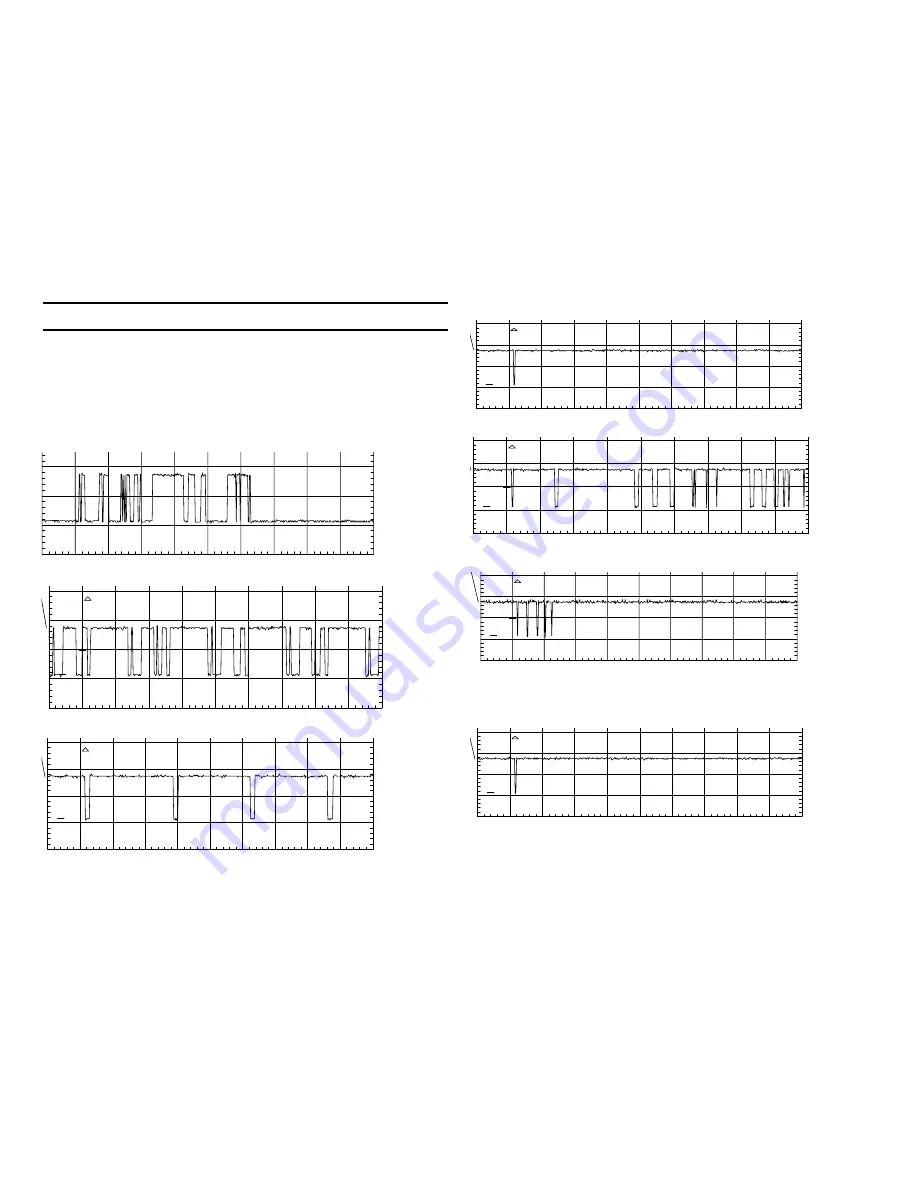
CE – IC202/pin 11 to Flash ROM IC205/6
STOP
CH1!2.00 V= MTB10.0us- 1.16dv ch1-
1
T
CS 3 – IC202/pin 8 to A/V Decoder IC401
CH1!2.00 V= MTB10.0us- 1.16dv ch1-
1
T
CS 4 – IC202/pin 7 to HGA IC601
CH1!2.00 V= MTB10.0us- 1.16dv ch1-
1
T
CS 2 – IC202/pin 9 to A/V Decoder IC401
CH1!2.00 V= MTB10.0us- 1.16dv ch1-
1
T
These last two chip select signals only appear at power ON and during
disc PB.
CH1!2.00 V= MTB10.0us- 1.16dv ch1-
1
T
XCS – IC601/pin 111 to ARP2 IC303
HCS - IC601/pin 118 to Servo IC701
CH1!2.00 V= MTB10.0us- 1.16dv ch1-
1
T
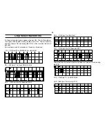
Chip Select Waveforms
All these chip select signals appear at power ON. The first five chip se-
lect signals also appear as long as the unit is ON. The last two only
appear at power ON and during the PB of a disc (or when the disc is
paused).
All waveforms are 3.3Vp-p taken at 10usec/div. time base.
CS 1 - IC202/pin 10 to SRAM IC204 / HGA IC601
Summary of Contents for DVP-S300
Page 4: ...1 NOTES ...
Page 13: ...10 NOTES ...
Page 19: ...16 NOTES ...
Page 25: ...22 NOTES ...
Page 29: ...26 NOTES ...
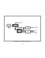
Page 35: ...32 2ND GENERATION OPTICAL ASSEMBLY SYMPTOM 3 1 3 01 19DVD03 ...
Page 39: ...36 NOTES ...
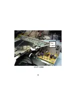
Page 61: ...58 Flex Cable DVP C650 ...
Page 71: ...68 NOTES ...
Page 76: ...APPENDIX ...

