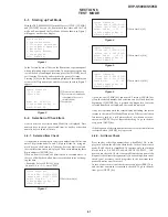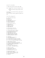
6-4
(6-6) Register in Decrypt IC (IC811)
Register write
→
Register read matching check
Error 05: Write/read data mismatch error
0x00 – 0xfc data (lower 2 bits are masked) are written to the inter-
rupt register, then read to check for matching.
If write/read mismatch error occurred, checking can be repeated.
(6-7) Reset of Decrypt IC (IC811)
Register write
→
Hard reset
→
Register read
Error 02: Reset error
05: Write/read data mismatch error
After “0xfc” is written to the interrupt register, whether it is ini-
tialized to “0x00” by the reset pulse signal is checked.
To make sure, the written data is read to check for matching be-
fore reset is executed.
(6-8) Interrupt Line in Decrypt IC (IC811)
ROM (IC803)
→
ARP (IC806)
→
Decrypt (IC811)
Error 22: Decrypt (IC811) interruption is not detected
AC-3 audio data stored in ROM (IC803) are transferred to the
Decrypt via ARP (IC806), then the reserved data interruption from
Decrypt (IC811) is detected.
To discriminate the ARP (IC806) interruption which is alsosent in
the same line, the ARP (IC806) interruption is allmasked.
(6-9) Reserved Data Head Byte Reading
ROM (IC803)
→
ARP (IC806)
→
Decrypt (IC811) reserved data
head byte read matching check
Error 05: Write/read data mismatch error
22: Decrypt interruption is not detected
AC-3 audio data stored in ROM (IC803) are transferred to the
Decrypt via ARP (IC806), then the reserved data head bytes are
read from Decrypt (IC811) register.
As this audio data consists of 5 sectors, 0, 1, 2, 3, 4 data are writ-
ten at the head of reserved data of respective sectors.
Whether these data are matched is checked through every sector
interruption.
If write/read mismatch error occurred, checking can be repeated.
(7) AV Decoder (IC203)
(7-2) Register in 64020
Register write
→
Register read matching check
Error 05: Write/read data mismatch error
“0x00” – “0xff” data are written to 51 registers where all bits can
be written/read, then they are read to check for matching.
If write/read mismatch error occurred, checking can be repeated.
(7-3) Reset Line in 64020
Register write
→
Hard reset
→
Register read matching check
Error 02: Reset error
05: Write/read data mismatch error
After “0xff” is written to the Capture/Compare Control Register
0, whether it is initialized to “0x00” by the reset pulse signal is
checked.
To make sure, the written data is read to check for matching be-
fore reset is executed.
(7-4) DREQ Signal Line in 64020
AV Decoder (IC203) DMA check
Error 03: Data write error
04: Data read error
05: Write/read data mismatch error
06: DMA transfer DREQ error
07: DMA transfer address error
The connection of DREQ signal line to the AV Decoder (IC203)
is checked through DMA transfer.
If no error is found in DMA transfer, the transferred data are com-
pared with the DRAM (IC810) data read from the register.
(7-5) DRAM in 64020
ROM data
→
AV Decoder (IC203)
→
DRAM (IC810)
→
AV De-
coder (IC203) read matching check
Error 03: Data write error
04: Data read error
05: Write/read data mismatch error
06: DMA transfer DREQ error
07: DMA transfer address error
ROM (IC803) patterns are copied to all areas to be checked. Be-
cause of large DRAM (IC810) capacity, each time 256 bytes are
copied, the addresses of copy source (ROM) are returned by 255
bytes. In detail check, to verify all bits in DRAM (IC810), the bit
patterns are checked again after inversion. DMA is used when
writing/reading the data. Though the bus width of AV Decoder
(IC203) is 64 bits, the display is given in 8 bits. Namely, actual
address is 1/8 of displayed data, and lower 3 bits indicate the byte
position.
Overwriting by the shadow can be detected, as the data are written
to all areas, then read. In the detail check, all areas of RAM are
checked twice by inverting the data, while in the simple check one
block is checked, then subsequent 4 blocks are skipped, and also
inverted data are not checked.
If write/read mismatch error occurred, checking can be repeated.
Summary of Contents for DVP-S500D
Page 12: ...1 2 ...
Page 13: ...1 3 ...
Page 14: ...1 4 ...
Page 15: ...1 5 ...
Page 16: ...1 6 ...
Page 17: ...1 7 ...
Page 18: ...1 8 ...
Page 19: ...1 9 ...
Page 20: ...1 10 ...
Page 21: ...1 11 ...
Page 22: ...1 12 1 12 E ...
Page 52: ...7 5 E 1 2 10 12 14 24 25 CN252 MB 78 BOARD Side B ...


